Version 2 Battery Charger and Boost Regulator

PCB-V2

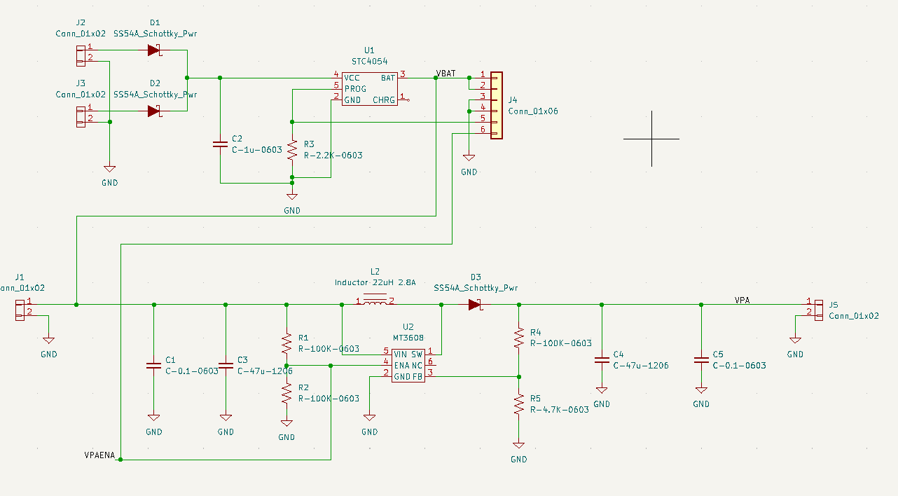
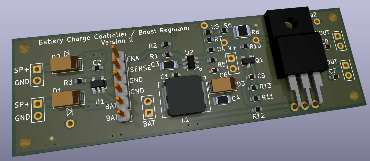
After blowing up the transmitter power amplifier (1W) one too many times during test, I decided that it would be useful to put a current-limit circuit on my Charge/Boost board.  This board takes the power from two 1W solar panels, and uses that to charge the Li-ion battery in a controlled manner.  The battery powers the Drift Buoy and, through a switching boost converter provides 13V to the transmitter amplifier stage.

The Class-E transmitter amplifier is sensitive  to loading, and a badly-matched load can cause excessive power dissipation or over-voltage in the transistors.  In the process of trying to determine the safe limits for the amplifier I’ve managed to smoke a few transistors.

So the new regulator design now includes foldback current-limiting.  I’ve added more test points and several configuration options to this board (not all parts will be stuffed at the same time), allowing for easy experimentation.  The previous board had two layers, but this one uses four.  The additional cost is minimal and this allows for a much nicer layout.

The current-limit won’t protect the Class E amplifier under all circumstances, because the amplifier efficiency is due to the careful phasing of transistor voltage and current.  Different loads (resistive and reactive) will cause both amplitude and phase shifts of the voltage and current at the transistor so even with current-limiting there can be excessive transistor dissipation.  Current limiting will help but I also have a big bag of transistors.  And they’re cheap: about  17 cents each.

I should have test results in a couple of weeks.


SWR Bridge

I finally put the components on the SWR bridge board:

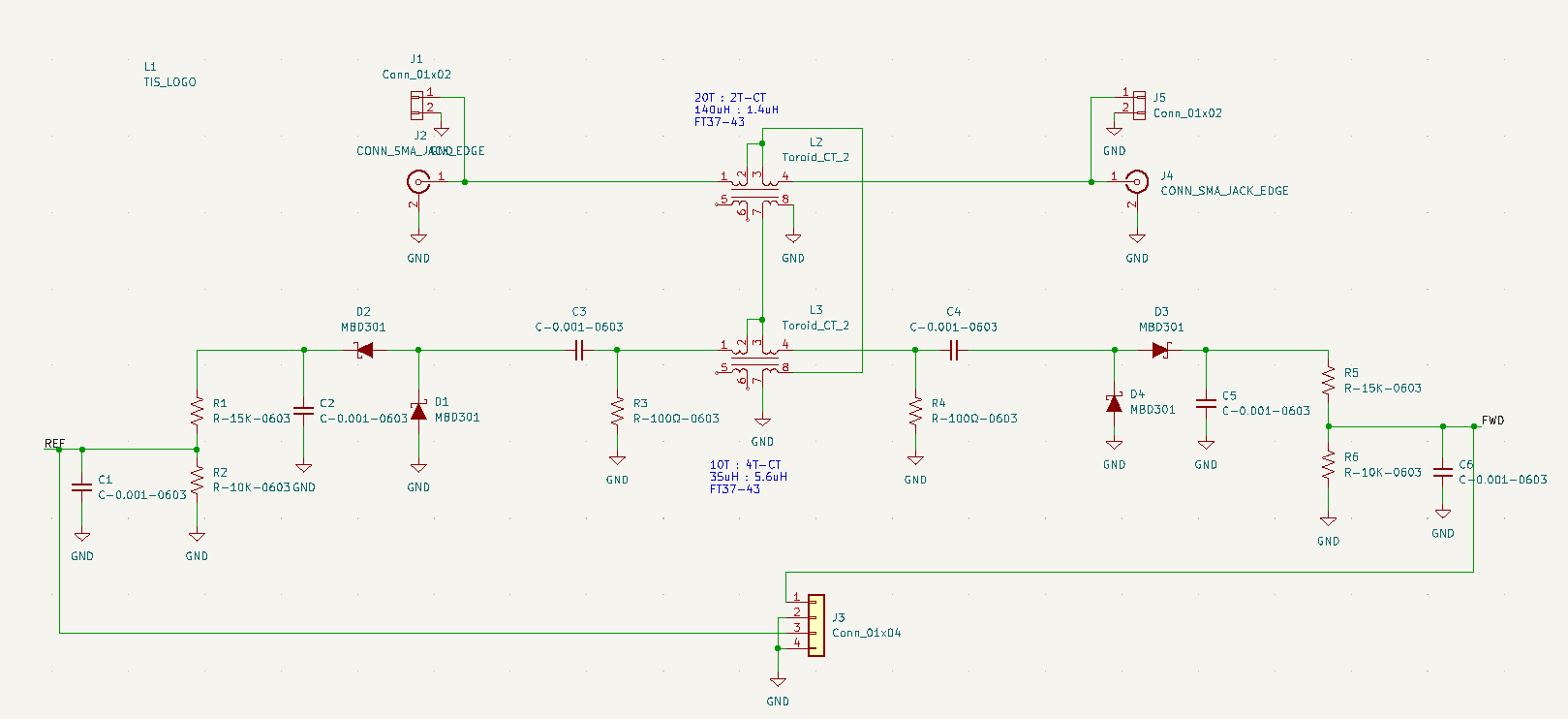
SWR SchematicSWR Bridge Schematic

The SWR bridge uses a common two-transformer directional coupler design, and should have very low excess loss.  Typically the coupled taps are designed for a 50 Ohm impedance, which makes perfect sense if you want to connect it to other test equipment.  But here we are using a full-wave rectifier diode detector design, and we can reduce the loss, or increase the sensitivity, by scaling up the impedance at the coupled ports.  Here I adjusted the transformer turns ratios to drive a 100 Ohm load at the detector ports.

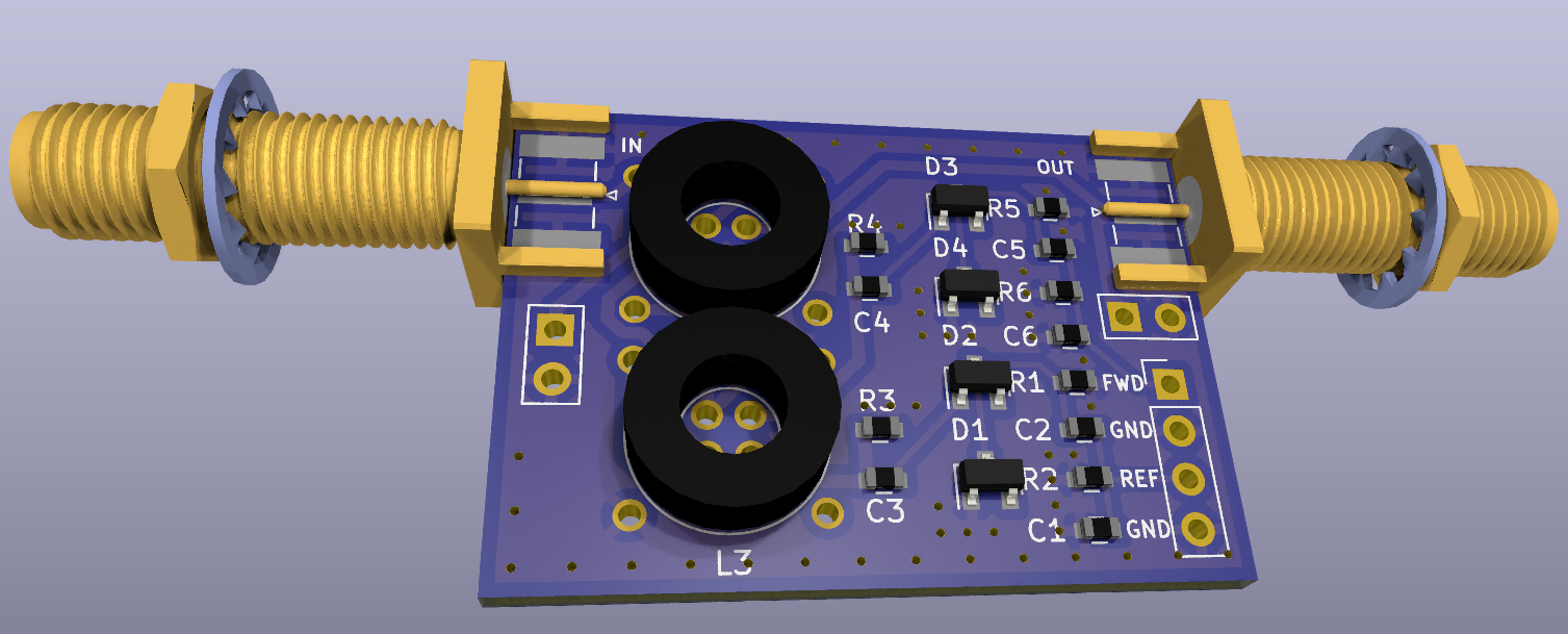
SWR-3D3D KiCad Rendering

 It turns out that there is a downside to how quick/easy/cheap the design-to-PCB process is.  First, I spent some hours simulating various circuit options in LTSpice  Then, using KiCad for schematic capture and circuit-board layout,  I had the schematic and PCB design finished in one evening.  This included building some custom symbols and footprints for my toroid coils and the Schottky diodes I had chosen.  That same evening I sent the PCB files over the internet to JLCPCB, and selecting the next-to-cheapest delivery option I had five boards fabricated and shipped for $12.80.  Complete(!)  These were two-layer boards, but four-layer are only very slightly more expensive.  Since the component count was low, I chose to not get the stainless solder-paste stencil, but those are also quite inexpensive and certainly worth it if you have a more complicated board.

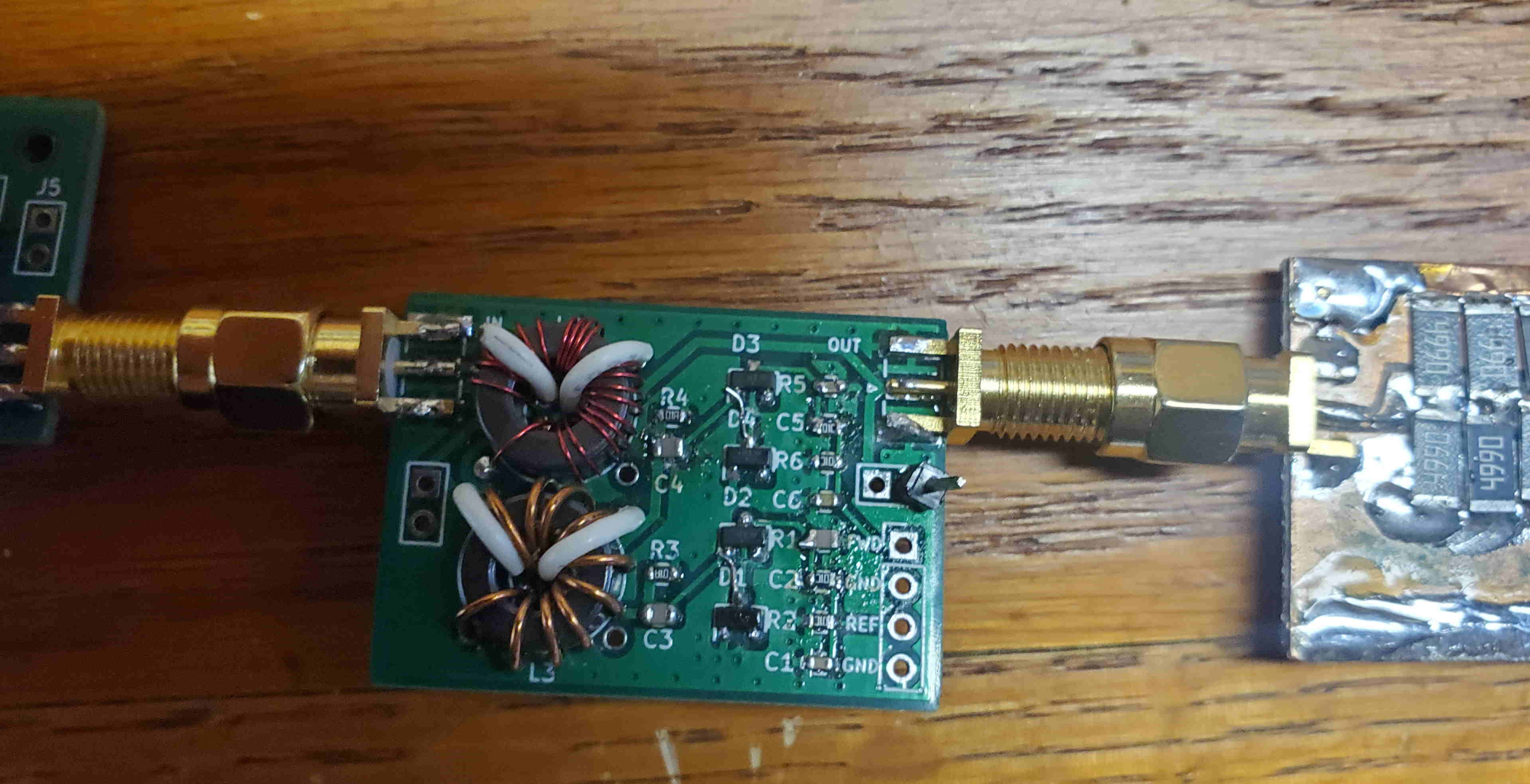
So what’s the downside?  It’s so easy, quick, and cheap that I  perhaps don’t spend enough time checking my work.  Turns out I had four silk screened reference designators swapped (which meant I installed those parts in the wrong location), and I had screwed up the location of two diodes in my original schematic.  Fortunately, all the traces are on the top side, and it was easy to cut traces and solder wires to fix that little SNAFU.

PCBBoard Under Test (with cuts and bodge-wires)

 With those fixes I was able to test the SWR detector with my signal generator at +20 dBm (1/10 W), and using my Drift Buoy amplifier at +30 dBm (1 W).  I was able to test with SWR of 1:1, infinity,  1.27:1, and 1.168 (these last two using a 10dB attenuator with open and shorted outputs).  I’m going to have to do more measurements at different SWRs.  I will be measuring the forward and reverse detector output voltages with the Drift Buoy A/D converter, and since the diodes are non-linear, will need to characterize the behavior at different power levels and SWR values.

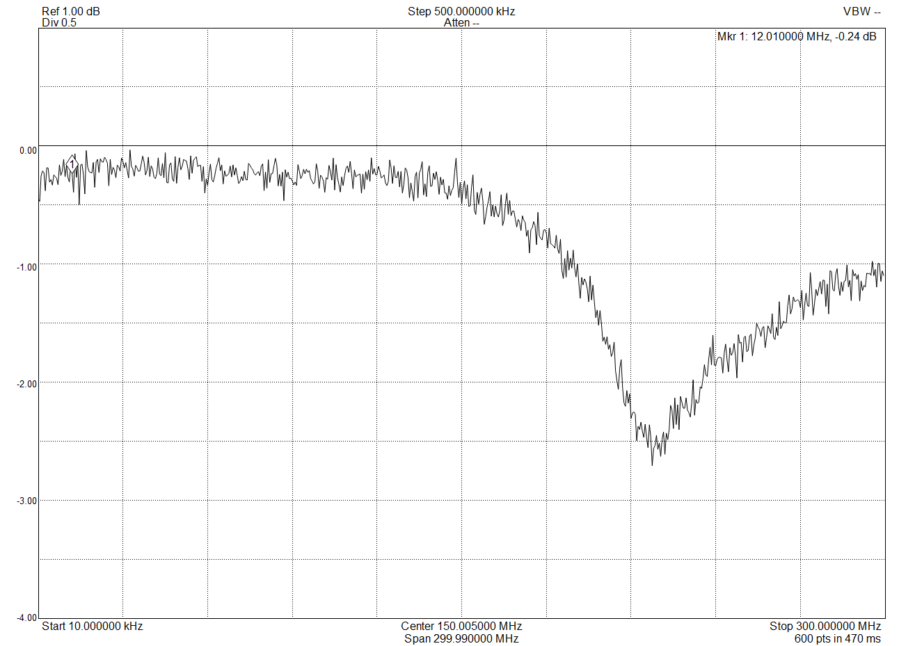
loss2Through-Loss (-0.2dB @ 10 MHz)

 The last test was a loss measurement using my spectrum analyzer and tracking generator.  I hadn’t been too concerned about behavior far away from the 10 MHz frequency of operation, but it looks like the SWR bridge behaves well beyond 100 MHz.  The loss at 10 MHz is about 0.2 dB, which is pretty good.

By the way, those white wires on the toroids are the two-turn center-tapped windings.  I used a trace on the PBC for the center-tap connection and use two hairpin wires for the turns.


Battery Charger / Boost Regulator

As mentioned, I still needed to build the Li-Ion battery charger / boost regulator board.

Schematic

This charger circuit takes the output from two 1W solar panels and uses that power to charge the Li-Ion battery.  The charge-controller is not an MPPT design, just a linear regulator with other features.  But the solar panel output voltage fairly well matches the Li-Ion requirements, so not enough power is wasted to justify using a more complicated circuit.  The charger provides a signal output that indicates the charging current,  and the Buoy controller monitors this and the battery voltage so we should have a good idea of the battery state.

The boost converter input comes from a Li-Ion battery, nominal voltage 3.7V to 4.2V.  The output is 13.4V, nominal load about 100mA (this powers the Buoy 1W 10MHz power amplifier.

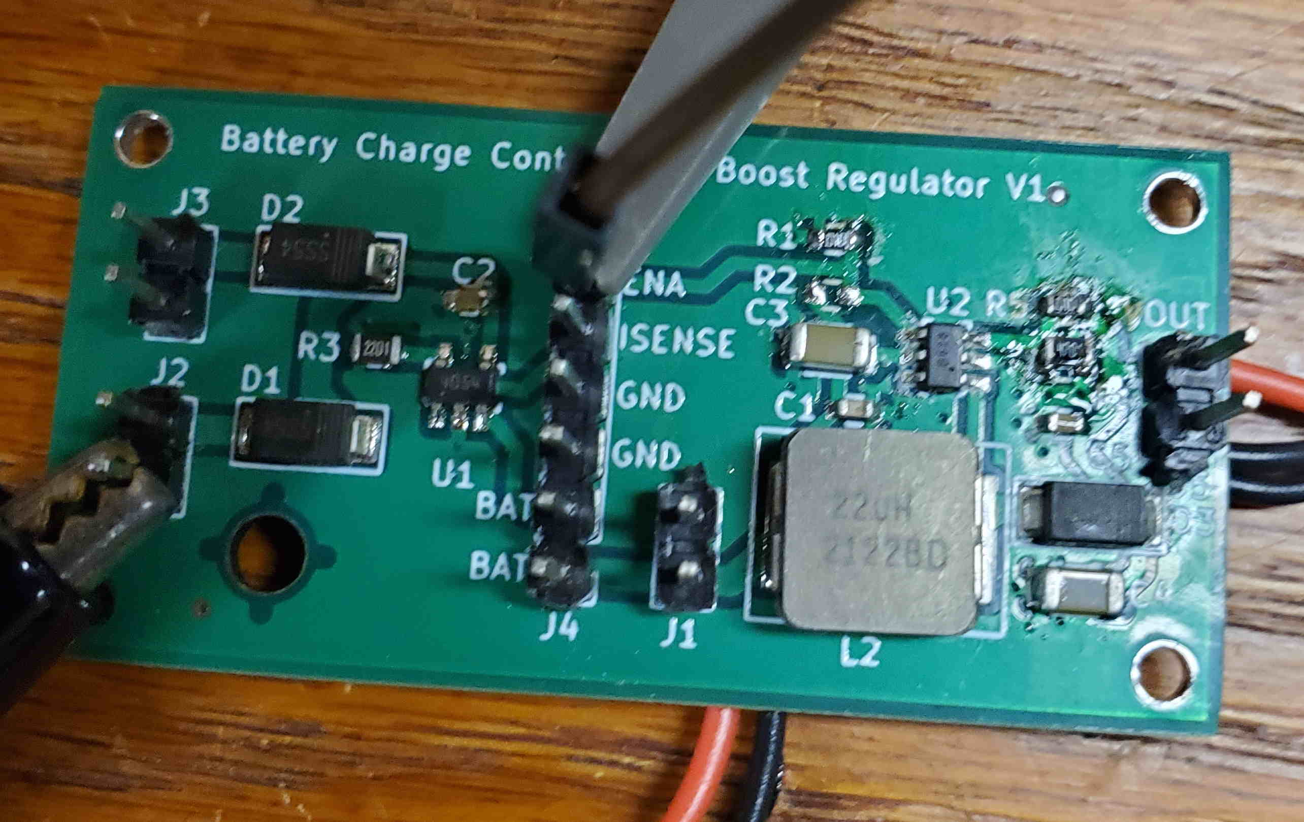
So, I collected the components, dabbed solder-paste on the PCB, hand-placed the parts, and put it in my converted toaster-oven reflow oven.  It came out great, but I discovered that I had four resistors mis-identified on the silkscreen. I also was missing a couple of the resistor values so I had to to substitute some that were physically too big.  The completed boards looks good, except where I had to hand-solder to correct my mistakes:

test-2(I need to clean off that scorched flux!)

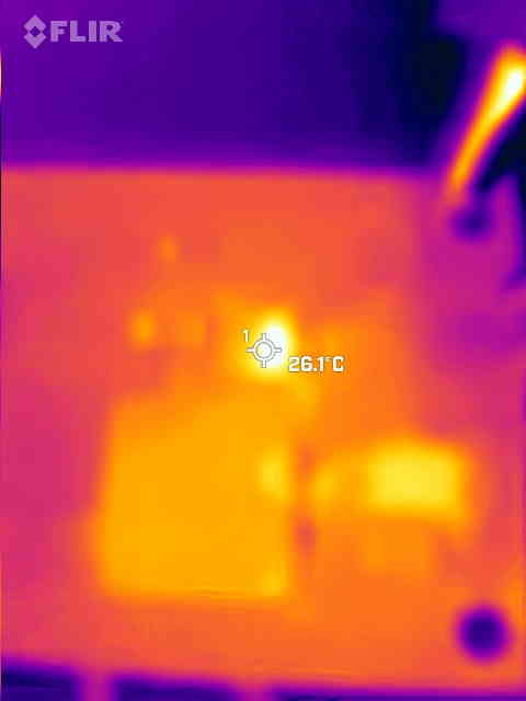
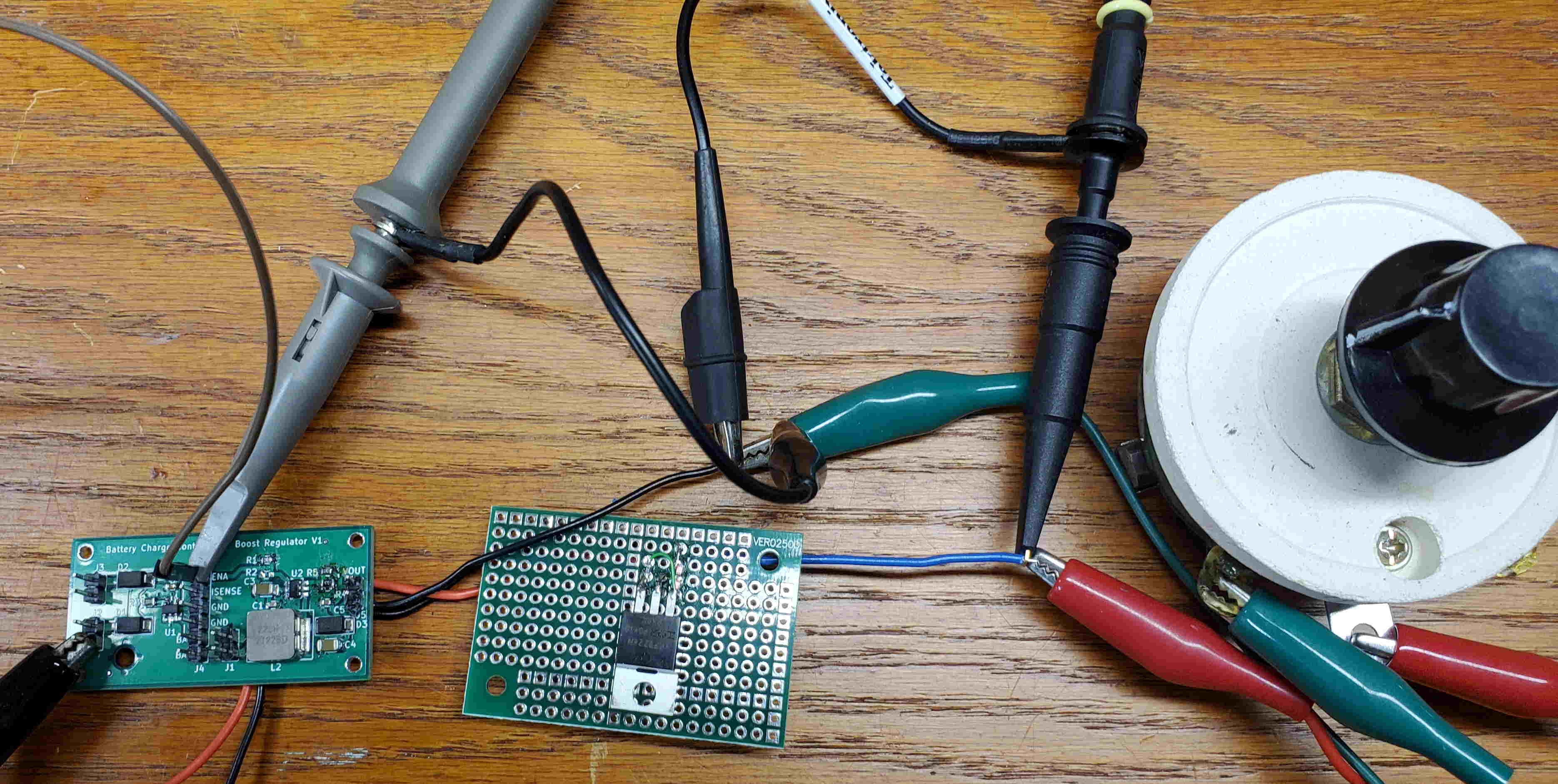
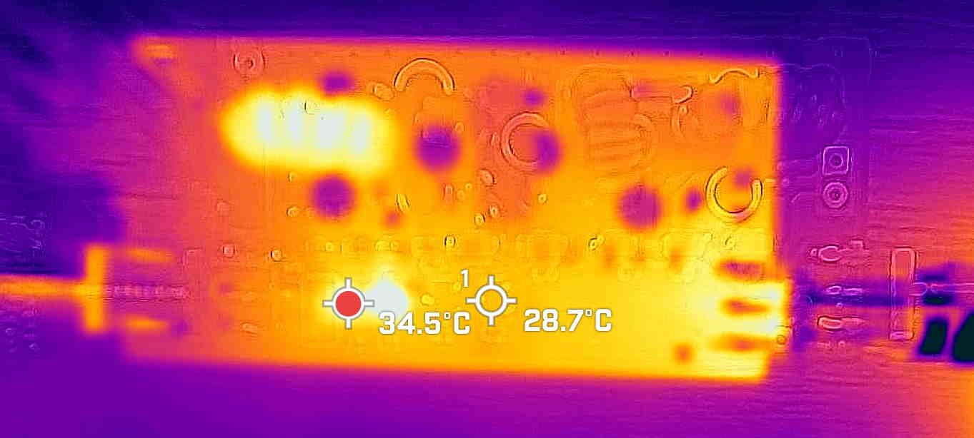
I hooked it up to some test gear and put the boost converter through its paces.  I measured about 87% efficiency for the converter, and only a few degrees temperature rise for the components:

test-3Thermal Scan

test-1Testing the boards

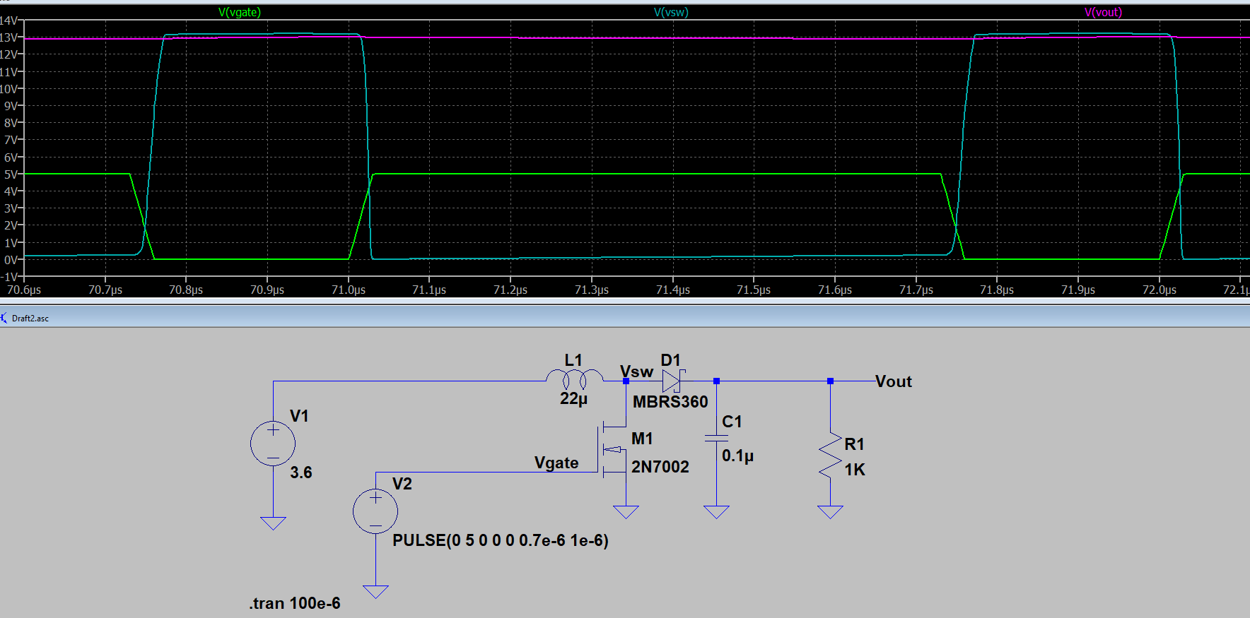
See that little perfboard with the transistor?  That fixes a problem with my overall design.  The boost-converter chip has an enable pin, and I am planning to use that to get software control of the amplifier power.  Well, the converter shuts down, but even then the Li-Ion battery voltage still sneaks through the converter circuit (through the inductor and diode), applying about 3.5V to the amplifier:

SW1Essential Boost Converter Circuit

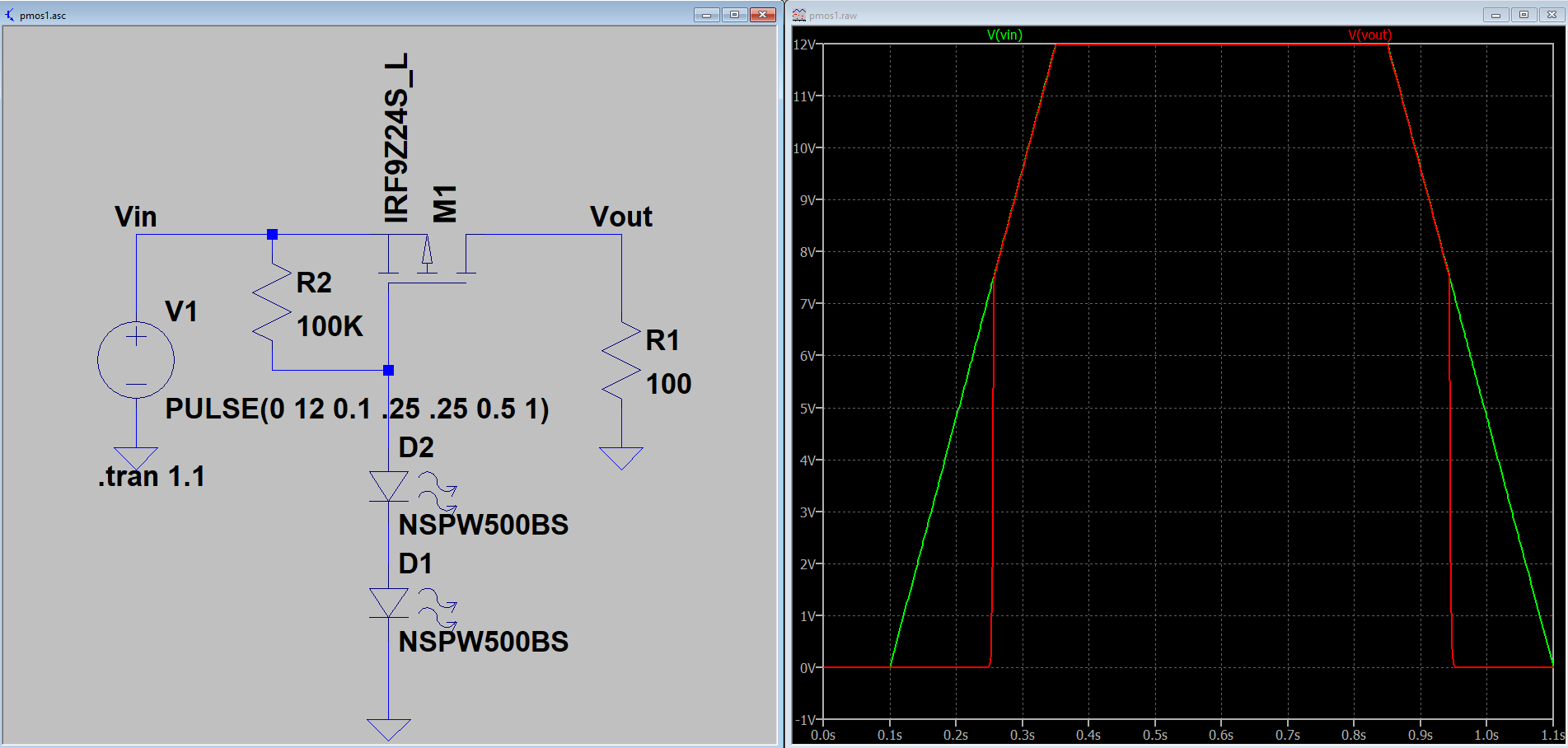
I ended up inserting a PMOS FET switch between the converter and the amplifier, which disconnects when the input is under 5V.  It works quite well, and those two LEDS used as low-voltage Zeners, (sort of) gently glow when power is applied (about 0.1 mA through the LEDs):

PGateLow-Voltage Shutoff Circuit

I’m not done with this board yet, I still need to test the solar panel and charger circuit.  I was worried about that boost converter ripple (it switches at about 1MHz) getting into the transmitter output.  I’ve got LC filters on the power input, but is that enough?

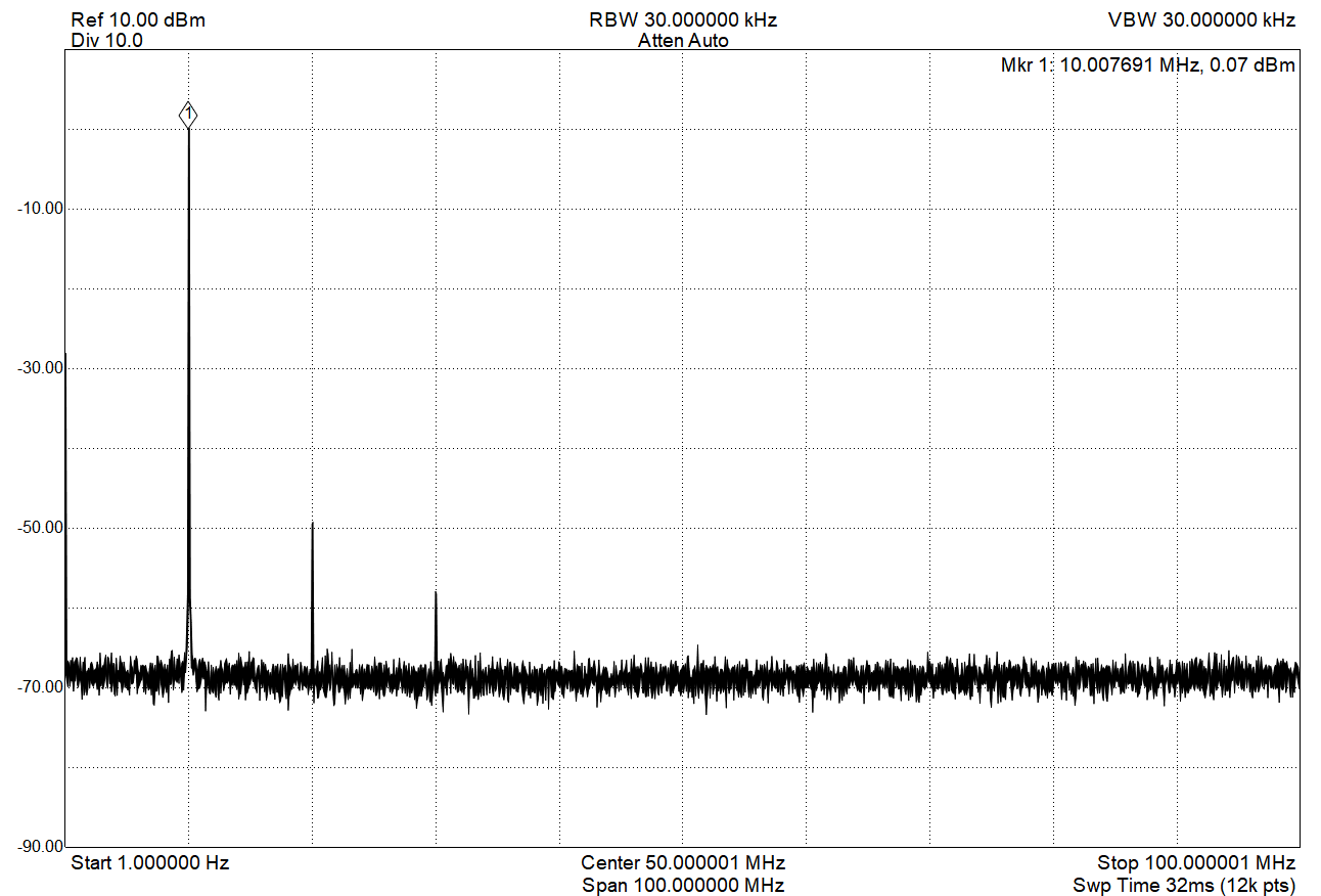
Good news: testing shows no detected switching-related spurs above my -80dBc noise floor.


Drift Buoy Preview

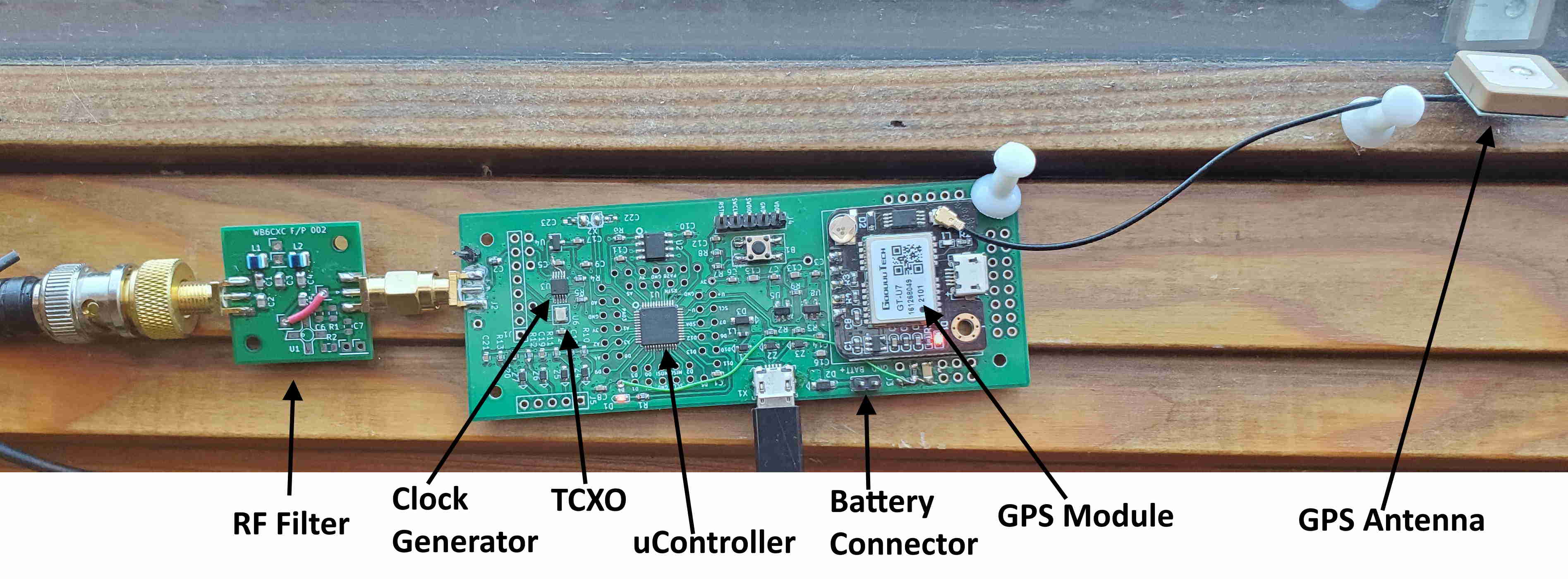
The Drift Buoy project is much like sailing is for me:  The destination is quite secondary to the journey.  But in addition to enjoying the scenery along the way, I have also been making progress on actually building the thing.  Here is some evidence:

ControllerThe Buoy Controller

control board 1Buoy Controller Under Test

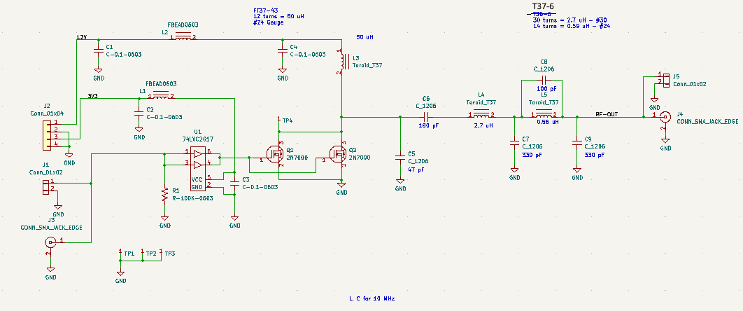
V0.2-Schematic1W Class-E Power Amplifier

V0.2-3DPower Amplifier


Thermal V2
Power Amplifier Under Test (thermal measurements)

Rev 2 OutputPower Amplifier Output Spectrum (with 30dB attenuator)

I still have two more PC boards waiting for me to build and test; a little power/SWR bridge that will be monitored by the Buoy controller, and a solar panel-input battery charger, combined with a 3.7V -to- 12V boost switching regulator (for the amplifier power supply).

I’m also probably going to hack a wireless NRF24L01 transceiver module onto the controller, giving me the ability to remotely access the controller debug interface (up to about 100 meters distance).  This will not be activated when the buoy is actually at sea, but will let me keep tabs on things when the buoy is floating close to home.

I will be providing details here, covering the more interesting (I hope) aspects of the Buoy.


Fractional (and other) Dividers

Since I am so enthusiastic about the fractional dividers used in the Si5351 (and about fractional dividers in general — in my career I’ve designed these into many telecommunications projects), I thought it appropriate to describe some details.

There are many types of dividers used in frequency synthesis and clock generation.  The basic “divide by N” counter will take an input clock and output a clock at the frequency of (input / N).  N can be any integer.  This works well if you want to generate (say) a 2 MHz clock from a 10 MHz input — just divide by 5.  But if you want to generate a 4 MHz clock, or a 1.875 MHz clock you just can’t get there from here using a plain divide-by-N.

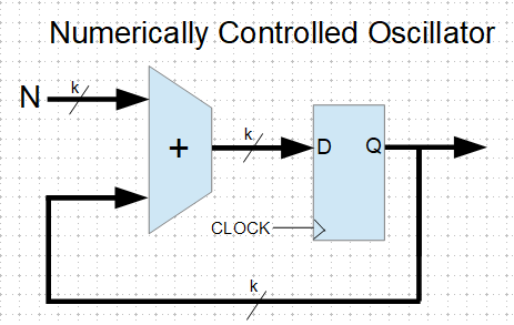
Another divider commonly used in communications design is the Numerically Controlled Oscillator (NCO), which is essentially an adder and an accumulator (register bank).
NCO

The adder takes the accumulator output and adds a constant value (the addend “N”), the sum going back into the accumulator.  The accumulator overflows once per output cycle.  If you wanted to generate that 1.875 MHz signal from your 10 MHz clock, you could use a 4-bit NCO, with the addend = 3.  This gives you a division of 16/3, and an output frequency of 1.875 MHz.  With this 4-bit NCO you can get ratios of 1/16, 2/16, 3/16 … 7/16, 8/16.  Interestingly though, you can’t divide by 5, you can only divide by (2^k)/N, where k is the size of the accumulator.  If you increase the size of the NCO you can get arbitrarily close to any desired fraction, and NCOs of 32-bits and larger are common.

The NCO also has the useful feature of providing a parallel output that can be used to drive a sine (or other function) lookup table, which can be used to generate low-distortion, low-jitter signals.  Modern function-generators and radios usually use NCOs for this reason.

But sometimes you just need (or want) to divide precisely by some arbitrary number that isn’t limited to an integer or related to a power of two.  Or, you don’t need the parallel output of the NCO.  This is where the fractional divider (FD) comes in.  There are ways to work around this NCO divisor limitation by dynamically altering the addend, but this complication may not be warranted. The FD has a shorter datapath and uses fewer gates than the NCO, which translates to higher speed, lower power, smaller chip area, and lower cost.  It can fit and operate where NCOs just don’t.

The fractional divider is sometimes called a “clock-dropping” divider.  For example, to divide by 2-1/2 (or 5/2), the FD will divide by 2,3,2,3,2,3…    frac 5,2

To divide by 3-2/3 (or 11/3) the FD divides by 3,4,4,3,4,4…frac 11,3

Dividing by 8-1/2 (or 17/2) gives this output:frac 17,2

You can see that the output signal is “stretched” by one clock-cycle at a regular rate.  This stretching, or dropped-clock, causes jitter, or frequency modulation of the output clock, which may need to be filtered out.  In the “8-1/2″ example above, with a 10 MHz input the output is 10 MHz / (8-1/2), or 1.17647xxx MHz, and the  repeating “8,9,8,9″ pattern  at the output creates a frequency modulation of 1.17647xxx MHz / 2.  The Si5351 uses a delay-line interpolator on the output FD which very effectively cleans up this jitter modulation.  The jitter from the FD used in the Si5351 PLL is attenuated by the PLL loop filter.  In other FD applications this filtering can often be performed by a simple bandpass filter.

For what it’s worth, sometimes with an NCO we want to use only the most-significant bit, and in this case there will also be this type of dropped-clock jitter.  That’s just a fact of life with a purely synchronous design.

Extreme frequency resolution is a powerful feature of the fractional divider.  For example, take the divide value of 8+25/100. This is of course equal to 8.25 .  But change the fraction to 8+32/127 and we get 8.251968xxx.   The fraction 8+31/123 equals 8.252032xxx. Since the Si5351 allows for numerator and denominator values up to 1,048,575 there is the potential for extreme precision.  Look up the “Farey Sequence” for more information on the resolution of fractions.

There are many ways to implement a fractional divider.  Here is a version designed in Verilog, which is a language used to design logic to be synthesized into an FPGA or other ASICs.  This design uses an 8-bit counter, which can generate any ratio  N/D, where (1 < D < 64) and (1 < N < (D / 2)).

module frac(
	input clk,
	input rst,
	input [7:0] b,
	input [7:0] c,
	output reg q
	);
	
	reg [7:0] sr;

	always @(posedge clk) begin
		if (rst) begin
			sr <= 8'b0; 
			q <= 0;
			end
		else if (sr[7]) begin
			sr <= sr + b;
			q <= ~q;
			end
		else sr = sr - c;
		end
endmodule

I have based this design on the “Bresenham line-drawing algorithm”, which was originally a very clever way to draw sloping lines on a graphics display without needing to use floating-point math.  This algorithm has proven useful in many other fields, including clock synthesis.

The fractional divider is flexible, simple, fast, and easy.  So the next time you want to divide a clock by pi, just use a 355/113 fractional divider. That gets you to within 8·10−8 .  Or if that’s not good enough, use 833719/265381 for better than eleven digits accuracy.
FSK with the Si5351 Clock Generator (Increasing the Si5351 register update rate)

The Si5351 spec sheets are complicated and confusing, but in the Arduino universe there are many libraries available for the it.  I started out with the Adafruit one, but have modified it to better suit my needs.  Several modifications were required to allow register updates at my 2.4 KHz interrupt rate.  Others were required, or desired, to clean up some other issues.

Speed-ups:

  • Increase the nominal Arduino I2C rate from 100 KHz to 400 KHz (the Si5351 supports a 400 KHz I2C rate).
  • The Adafruit library uses individual I2C “write single byte” operations, requiring that the I2C bus start, send an address byte, a data byte, and stop per each byte written.  Instead, where possible I use the I2C “burst write” mode which greatly reduces the number of I2C cycles when updating a register bank.
  • When only the PLL “B” numerator is changed, we don’t have to update all the PLL divider registers.  This speeds up the update.

Not particularly speed-related, but the Adafruit library performs a PLL reset when the dividers are updated.  This is not necessary, and creates frequency glitches.  I removed the reset operation when updating divisors.  This also does speed things up a bit.

Not speed-related, but the Adafruit library uses floating-point when calculating the fractional divider register values.  No doubt this is because the Si5351 app note shows the use of the floating-point “floor()” function in the calculation, but this is not required.  When the calculations are performed in the proper order, simple integer math is completely accurate.

Here is the gist of the code I use to update the PLL divider numerator.  Note the use of floor() in the original Adafruit comments (sorry about the line-wrapping):

void setupPLLnumerator(si5351PLL_t pll, uint8_t a, uint32_t b, uint32_t c) {
 
  uint32_t P1; /* PLL config register P1 */
  uint32_t P2; /* PLL config register P2 */
  uint32_t P3; /* PLL config register P3 */

  /* Feedback Multisynth Divider Equation
   *
   * where: a = mult, b = num and c = denom
   *
   * P1 register is an 18-bit value using following formula:
   *
   * 	P1[17:0] = 128 * mult + floor(128*(num/denom)) - 512
   *
   * P2 register is a 20-bit value using the following formula:
   *
   * 	P2[19:0] = 128 * num - denom * floor(128*(num/denom))
   *
   * P3 register is a 20-bit value using the following formula:
   *
   * 	P3[19:0] = denom
   */


   uint32_t f;
f   = (128 * b) / c;

    // build the registers to write
    P1 = 128 * a + f - 512;
    P2 = 128 * b - f * c;
    P3 = c;
	

	// since c (denom) hasn't changed, there's no need to write first two bytes// bytes to be written = 6
    uint8_t reg_bank[] = { 
      //(P3 & 0xFF00) >> 8,          // Bits [15:8] of MSNx_P3 in register 26
      //P3 & 0xFF,
      (P1 & 0x030000L) >> 16,
      (P1 & 0xFF00) >> 8,          // Bits [15:8]  of MSNx_P1 in register 29
      P1 & 0xFF,                   // Bits [7:0]  of MSNx_P1 in register 30
      ((P3 & 0x0F0000L) >> 12) | ((P2 & 0x0F0000) >> 16), // Parts of MSNx_P3 and MSNx_P1
      (P2 & 0xFF00) >> 8,          // Bits [15:8]  of MSNx_P2 in register 32
      P2 & 0xFF                    // Bits [7:0]  of MSNx_P2 in register 33
    };
	

  /* Get the appropriate starting point for the PLL registers */
  uint8_t baseaddr = (26); // PLLA
  
  i2cWriteBurst(baseaddr + 2, reg_bank, sizeof(reg_bank));
  
 
  return();
}

The timer-tick ISR runs at 2.4 KHz (416.66us). With these changes to the Si5351 library code, updating the PLL numerator takes 241us. The long Gaussian filter takes 50us per cycle, and the other operations in the ISR take less than 5us, so that leaves about 120us (per 2.4 KHz cycle) free for other program activities.  This is comfortably adequate, but trying to run the ISR at a faster rate might prove difficult.

For more information on using the Si5351 quadrature mode in radio applications, see this excellent posting by Hans Summers (QRP Labs): https://qrp-labs.com/images/news/dayton2018/fdim2018.pdf

Here is an alternate Si5351 programming library.  I was inspired to improve my I2C functions after looking at this one: https://github.com/etherkit/Si5351Arduino 

FSK with the Si5351 Clock Generator (Gaussian FSK)

Now that we know how to set the Si5351 to generate the FSK frequencies, we need to see about filtering (smoothing) the frequency transitions.

HF FM, using SSB:

  • Audio FSK signal modulates SSB transmitter, creating upper-sideband signal. This is identical to FM
  • Even with no explicit shaping, SSB transmitter audio filtering shapes the FM transient response
  • WSPR and APRS have no filtering
  • FT8/JS8 specify Gaussian filter, “BT = 2”, -3dB @ 12.5 Hz

With the Si5351 directly generating the transmit frequency there is no smoothing of the frequency shifts; the frequency change is a step function.  While this can still be received and decoded, the frequency steps create significant in-band interference:

FIR64 Gauss random 4FT8 spectrum with and without filtering

In addition, in some cases the receiver uses a filter that is matched to the transmit filter, and having mismatched filters impairs effective signal detection.

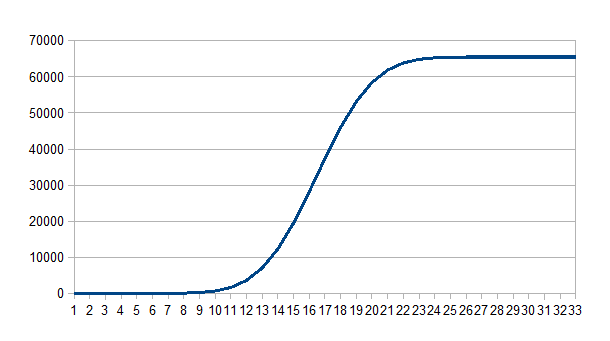
The filter specified for FT8 is a Gaussian filter.  This has a specific response, with characteristics that give good spectrum utilization.  These filters have a fairly gentle shape, smoother than a simple RC filter:

GaussianEGaussian Filter Step Response

Since we can’t use analog frequency-transition smoothing, we have to do this digitally, using small discrete frequency steps spread out over time.  The Si5351 divisors give us the small frequency steps, and the Drift Buoy software uses a timer-tick interrupt running at a 2.4 KHz frequency to chop the given Baudrate into many small timesteps.

The Gaussian filter runs at this 2.4 KHz rate and using the large frequency steps as an input, generates a smoothed sequence of small frequency steps, which are used to update the  Si5351 dividers.  This filter is implemented in software as a Finite Impulse Response filter (FIR).

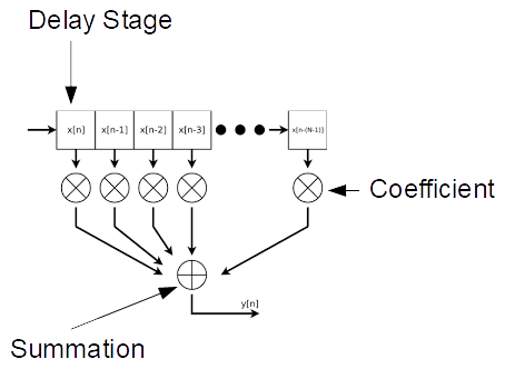
The “standard” FIR looks like this:

FIR-1

The input data is shifted through the delay-register chain, and at each shift the register contents are multiplied by the fixed coefficients and summed, giving the output.  Many different filter responses can be obtained by selection of coefficients.

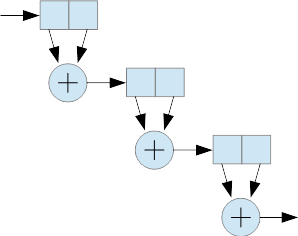
The Drift Buoy uses a simpler FIR structure, requiring no multiplications (there is one division operation for output scaling):

FIR-2

Each stage consists of two delay elements (these are 32-bit integer variables) and an addition.  Stages are cascaded as shown, and the resulting filter response is Gaussian.  The FT8 filter is clocked at 2.4 KHz and has 384 stages, which gives a -3dB response of 12.5 Hz.  The filter function takes about 50us per sample.

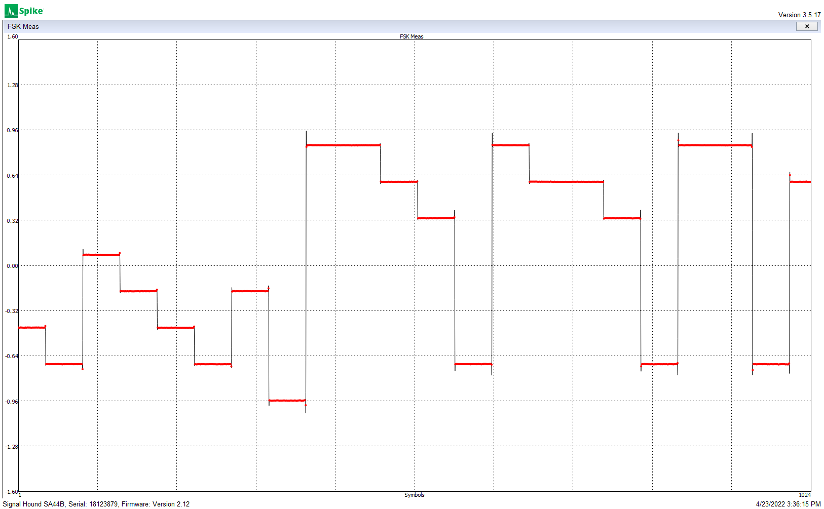
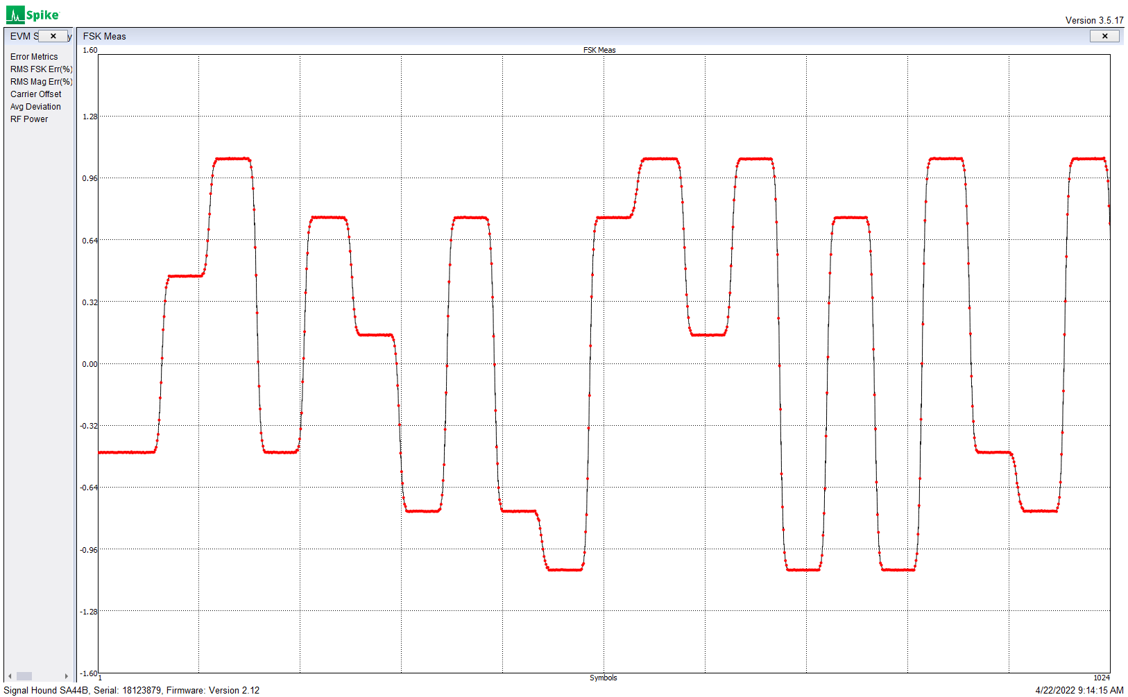
In the case of FT8, there are 40 available frequency steps from one of the eight tones to the next.  FT8 transmit data generates the eight tone values (0, 1, 2 … 7) . These are mapped to the values (0, 40, 80 … 280), which are sent to the filter.

RAW random 2

Unfiltered frequency steps

FIR64 Gauss rounded random 1

Gaussian filtered frequency steps


FIR256 Gauss Random 2

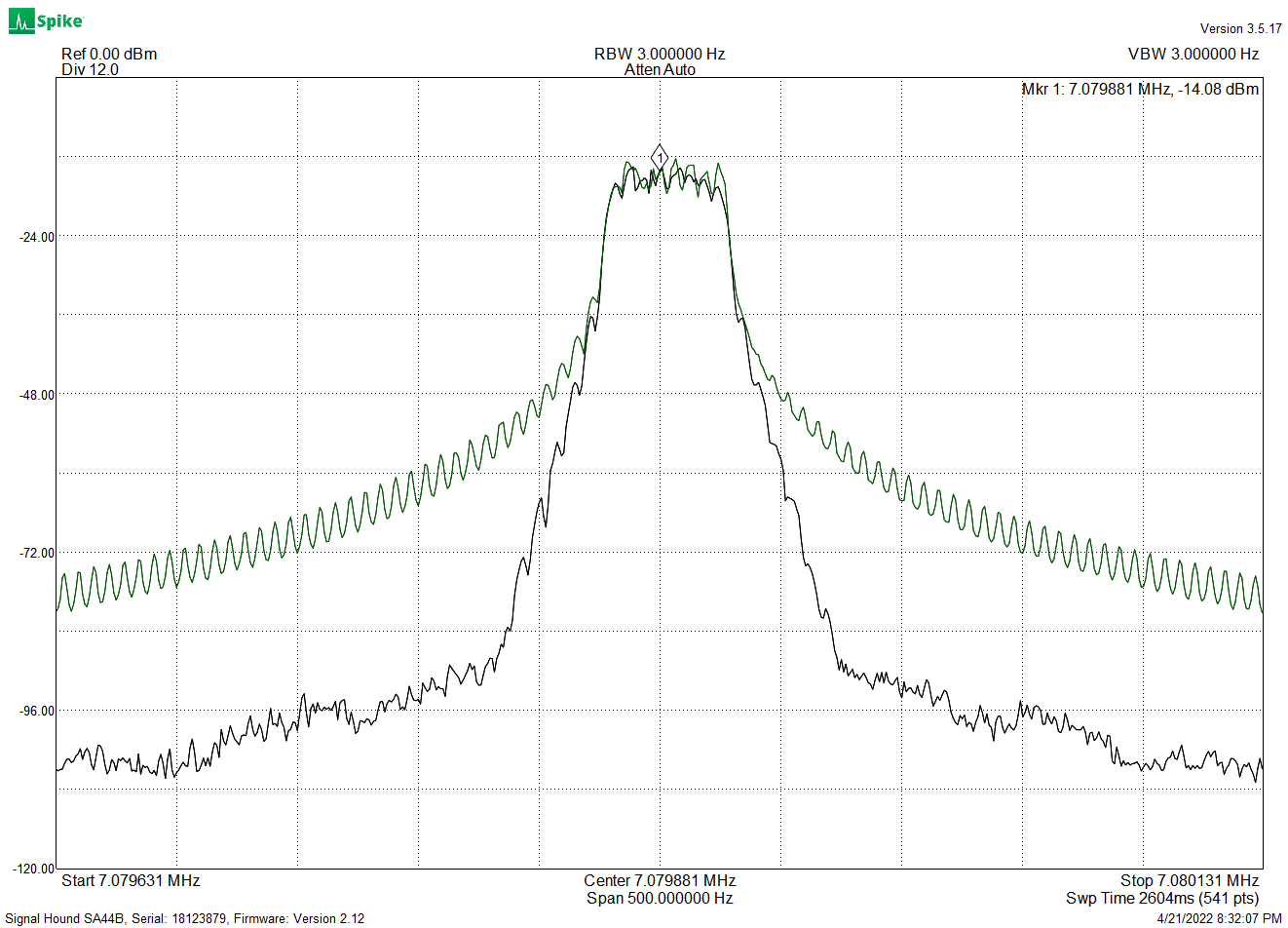
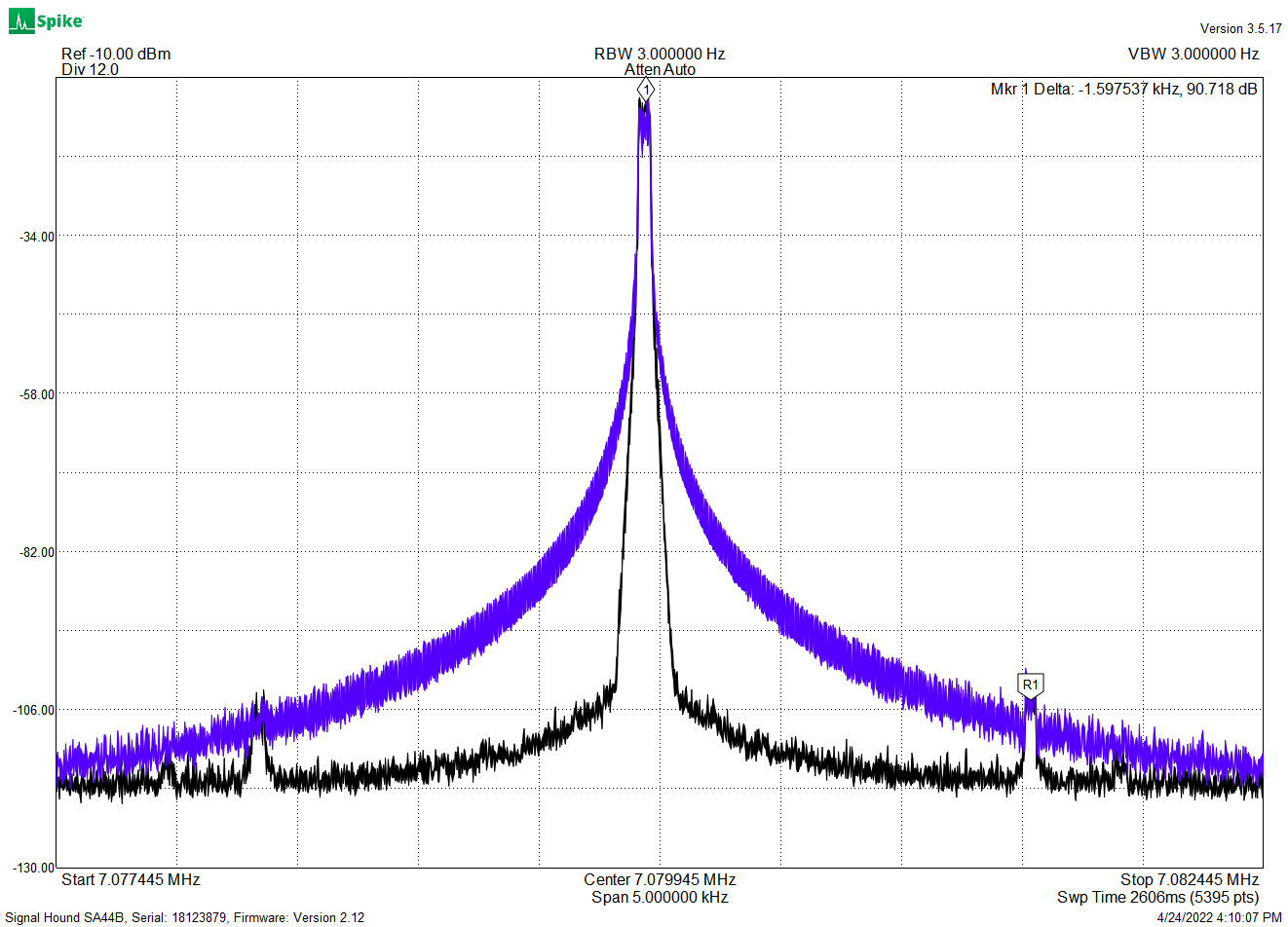
Unfiltered (blue) and filtered (black) 8-FSK spectrum,
showing 1,6 KHz sample-rate artifacts

 The above plot shows the performance of an earlier version of the FIR, which was running at a 1.6 KHz sample rate.  Increasing this rate to 2.4 KHz pushed the sampling artifact further out and reduced its amplitude.  Updating the Si5351 at the 2.4 KHz rate required speeding up the I2C interface and optimization of the register updates — more on this to follow.

While WSPR and APRS have no filtering requirement, for these modes the Drift Buoy uses a four-stage Gaussian FIR, clocked at 2.4 KHz, to provide filtering similar to the audio bandwidth of a SSB transmitter.

Next:

FSK with the Si5351 Clock Generator (Fractional Dividers)

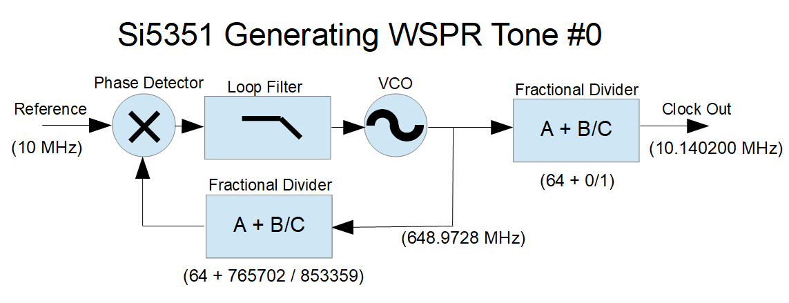
PLL

This is a simplified illustration of the Si5351, as configured to to generate the WSPR frequencies used in the  Drift Buoy design.

The reference comes from a 10 MHz TCXO, which provides acceptable stability.  The TCXO has an initial frequency accuracy of +/- 2.5ppm, which gives a +/- 25 Hz accuracy at the 10 MHz transmit frequency.  Better initial frequency accuracy and secondary digital temperature compensation can be achieved in software, but this is not necessary for Drift Buoy operation

The output divider is programmed to divide the PLL VCO frequency by 64 (no fractional component), which provides the cleanest spectral output.  The output divisor must be chosen so that the PLL frequency is within the available 600-900 MHz range. The FSK is done using the PLL feedback divider to vary the PLL frequency.

Determining the  PLL divider values is fairly simple.  We start by taking the desired output frequency (in this case 10.1402 MHz) and multiplying it by the output divider value (here, 64).  This gives us a PLL frequency of 648.9728 MHz.  We then take this PLL frequency and find the feedback divisor that will give us our reference frequency (here, a divisor of 64.89728 matches our 10 MHz reference).

So how do we set our “A + B/C” fractional divider to give us a ratio of 64.89728?  The “A” value is easy, that’s just 64.  We could set B = 897,728 and C = 1,000,000 — that would work, and setting C to one million makes the math easy.  But WSPR FSK tone spacing of 1.4648 Hz requires precise frequency control, and with a denominator of 1,000,000, incrementing the numerator by one gives a frequency change of 0.15625 Hz and you can’t get a 1.4648 step with that increment.  You can get close, probably close enough, but with a little math we can select divisor values that work much better.

Here’s a useful (very simple) equation for finding a PLL fractional-divider denominator when you are searching for a particular frequency step:

Fx = reference oscillator frequency in Hz,
OutDiv = output stage divisor.  This can be an integer or a fractional division,
Fdelta= desired output frequency step in Hz.
PLLdenom = PLL fractional divider denominator (the “c” in a + b/c)

Here’s the relationship.  Fdelta= Fx / (OutDiv * PLLdenom).

Rearranging this, we get:  PLLdenom = Fx / (OutDiv * Fdelta).

So for WSPR,  we have:

  • Fdelta = 1.4648
  • OutDiv = 64
  • Fx = 10e6

Which results in PLLdenom = 106669.8525

Since the “C” denominator can only hold integer values, we could round up to 106670, but we can do better.  The “C” value in the Si5351 fractional divider can be any value up to 1,048,575 (which is 2^20 – 1), so we can multiply this PLLdenom by 8, giving a rounded-up “C” of 853,359 (we could also multiply by 9 and still stay within the limits, but for some unknown reason I am using 8).  With this numerator we have a minimum frequency step of 0.18309996 Hz.  Incrementing the “B” numerator by 8 gives steps of 1.46479969 Hz — well within a microHz of the WSPR spec.  We will use these small steps later, when we do Gaussian filtering of the FSK modulation.

So what about the “B” numerator?  With B set to zero, the output frequency will be Fx * A  / (output divider), or in this case 10MHz * 64 / 64, or 10 MHz.  To get the desired 10.1402 MHz we need to set the “B” numerator to  (10,140,200 - 10,000,000) / 0.183099961, which equals 765702 (rounded).  Alternately, we can take the original 64.89728 divisor from our first calculation, and multiply the fractional part by  C/1,000,000 which also equals 765702 (rounded).

There are ways to achieve even finer frequency resolution, by changing both the “B” and “C” values — see the “Farey Sequence” — but the simple method used here requires only one parameter change, allowing for faster configuration of the Si5351 (more on that later.)

This example was for WSPR modulation, but the principles apply to the other FSK modes.


Next: FSK with the Si5351 Clock Generator (Gaussian FSK)

FSK with the Si5351 Clock Generator (Overview)

Si5351

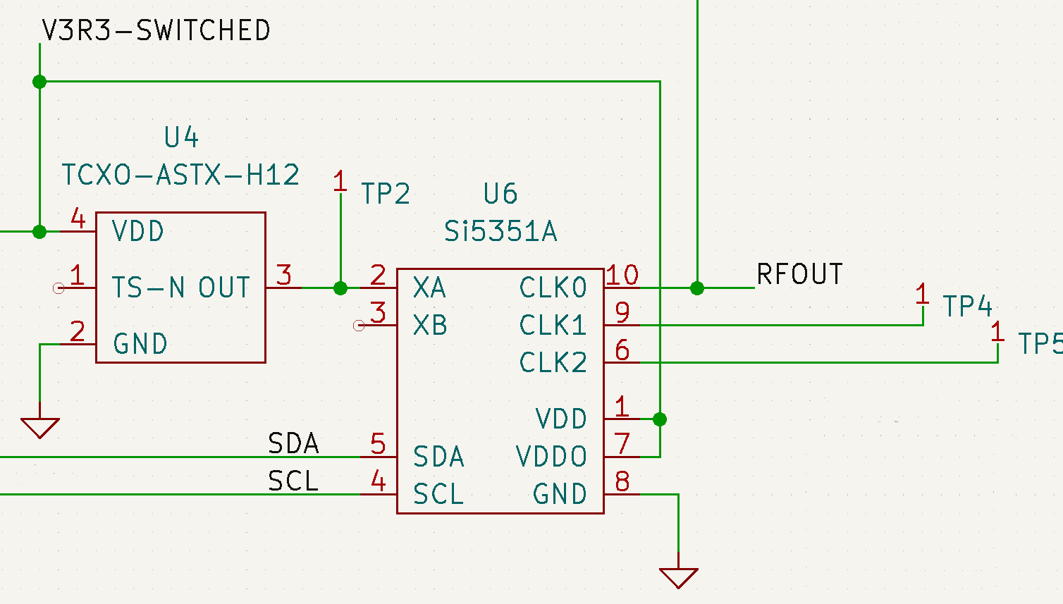
The Si55351 Clock Generator chip  is a real workhorse.  Give it a clock reference  (10 – 40 MHz), or a crystal (25 – 27 MHz) and it can generate three different output frequencies, between 2.5 KHz and 200 MHz.  There are two internal PLLs that can run from 600 MHz to 900 MHz, with fractional synthesis feedback dividers that can provide extremely high resolution.  Each of the three output pins is driven by a fractional divider, and a smoothing filter that significantly reduces the frequency transients caused by the digital dividers, providing quite a spectrally pure output for such an inexpensive device (about $1).  There are more features such as spread-spectrum dithering, and phase offset control (the phase offset can be used to drive quadrature modulator and demodulator architectures.)

With the fractional dividers used in both the PLL feedback and the three output stages, with some restrictions milli-Hertz frequency resolution can be obtained over the full frequency range.   Frequency accuracy is determined by the accuracy of the reference or crystal input. Configuration of the chip is done using a I2C interface.

In the drift-buoy I am using the Si5351 to generate the 30-meter (10.10 – 10.15 MHz) CW and FSK carrier frequencies.  The 3.3V logic level output of this chip feeds a small 1W class-E power amplifier, which drives a short whip antenna.  The FSK modes being used are APRS (2-FSK, 300 Baud, +/- 100 Hz), WSPR (4-FSK, 1.4648 Baud, 1.4648 Hz tone spacing), and FT8/JS8 (8-FSK, 6.25 Baud, 6.25 Hz tone spacing).

Given all the options and flexibility of the chip, there are many ways to generate a specific output frequency.  When generating the FSK frequencies there are many factors to consider.  In the following posts I will cover:

  • Selecting and setting the fractional divider values
  • Generating Gaussian Frequency Shift Keying
  • Increasing the Si5351 register update rate

Next: FSK with the Si5351 Clock Generator (Fractional Dividers)