I’ve been running a lot of designs through JLCPCB for both bare and assembled circuit boards, and I noticed that they were delivering aluminum substrate boards for quite reasonable priced. These have been used for front panels, but the thermal characteristics are great for higher-power devices such as LEDs. Interesting…
I’ve been using regular dummy loads in the testing of my WSPRSONDE (https://turnislandsystems.com/the-wsprsonde-v2-is-here/), but for easier testing I wanted a way to combine all eight channels outputs onto one 50 Ohm port. So I decided to try an aluminum substrate dummy load / attenuator / combiner:
40 dB is a good attenuation value when testing 1W signals: the combines eight outputs of the WSPRSONDE outputs the total is under 0 dBm, which is a safe level for my test equipment. So the circuit looks like this:
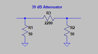
First, a single 40dB attenuator (actually 39 dB):
Combining eight of these stages to feed a single output:
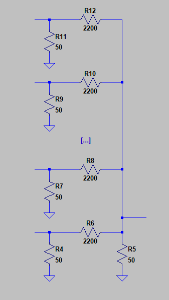
Note that the input port-to-input port attenuation is about 80 dB, which is good since I don’t want any port interaction.
The layout looks like this:
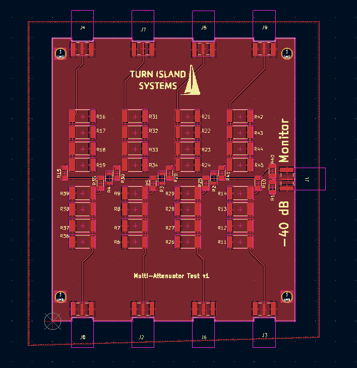
These aluminum boards provide only a top copper layer, with no through-hole capability. This makes ground plane connectivity a challenge. Here, I am relying on the edge-mount SMA connector ground pins to provide a bridge between otherwise isolated grounds. I also have three zero-Ohm resistors bridging across the horizontal trace where the eight attenuators are connected. As it turned out these jumpers were not needed, since the ground-current flows don’t normally cross this zone.
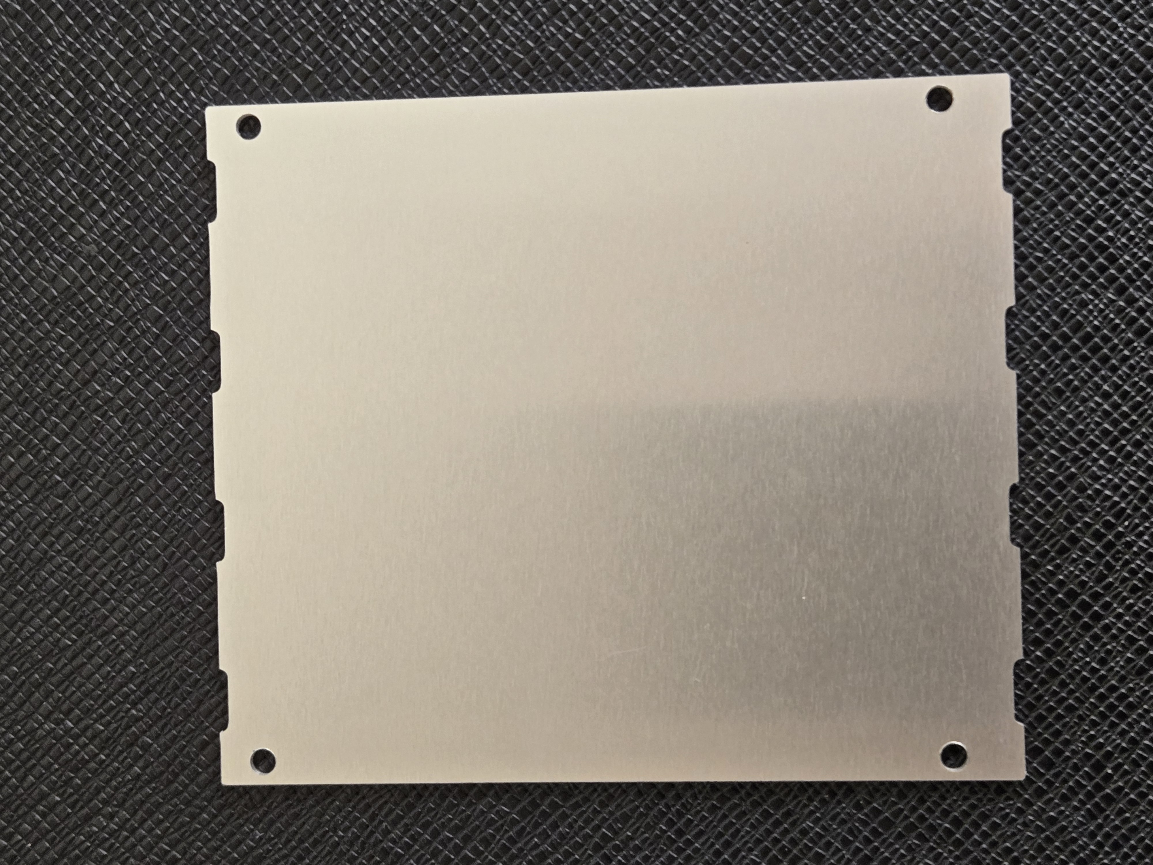
Here is the hand-assembled board. I use four 200 Ohm 2W resistors in parallel for each 50 Ohm load:
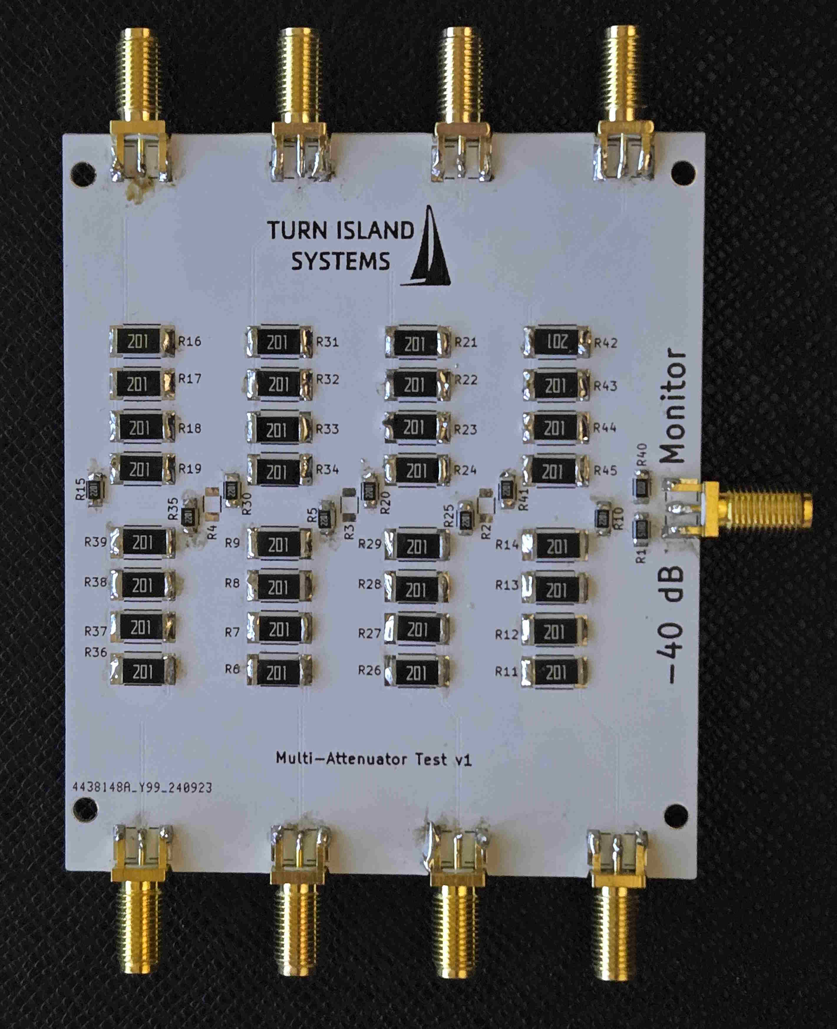
The back of the board is pure aluminum, and would be a good place to put a heat sink. At my <10W power levels, the heat sink isn’t necessary:
The dielectric constant of the insulation layer between the copper layer and the aluminum is not specified, but rumor has it that the capacitance has been measured at 0.56 pF / square mm. This does provide enough capacitance to the aluminum substrate for it to act as a ground plane at higher RF frequencies. I decided to not make a proper RF characterization board, but instead just try my dummy load design, using skinny traces so the characteristic microstrip impedance wasn’t *too* low. Since my frequency range of interest is between 1 and 50 MHz a sloppy design is unlikely to cause problems.
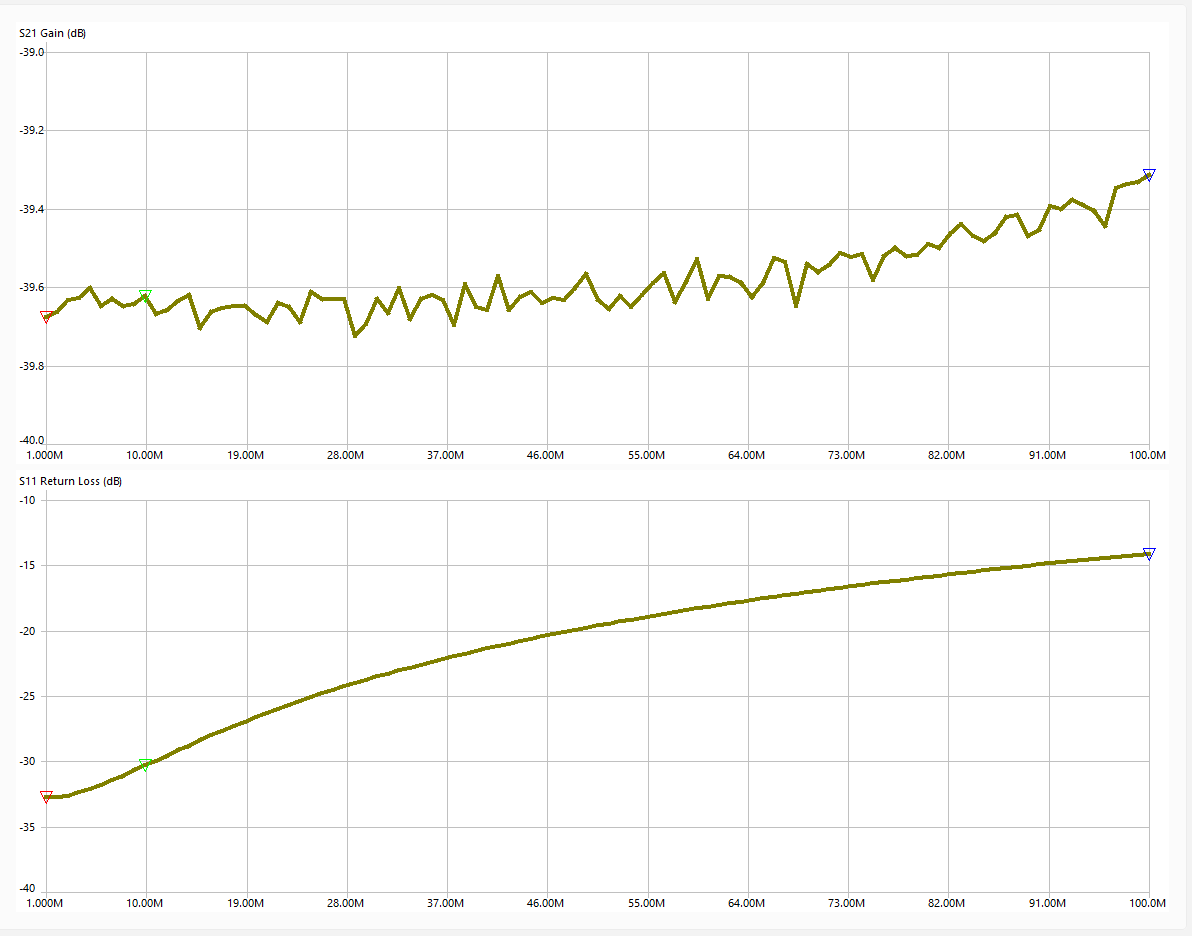
And it worked quite well! Here is a NanoVNA plot, showing the attenuation and return loss from 1 to 100 MHz. This is definitely good enough for my purposes.
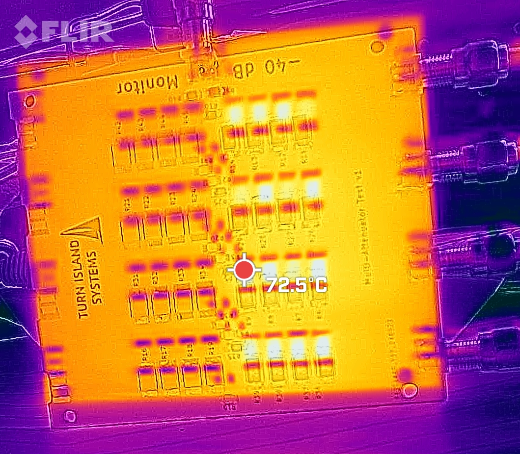
The thermal characteristics were quite acceptable too. Here is the board, only half-built, with close to 2W into each of the four ports. The resistors are showing about a +50 deg c temperature rise, which is well under the rating.
So, a successful result, and I now have a useful bit of test gear. It’s not a lab-grade GHz attenuator, but it certainly meets my needs.