Category Archives: Design Notes

Glitchless Power

TIS-1250 blue-small
The small NUC computers such as the Beelink series are incredibly capable and have become the computer of choice for RX-888 SDR receiver installations that run ka9q-radio and wsprdaemon software. But providing these small computers with glitchless power can be a challenge. The small switching power supplies used with these computers do not store enough power to maintain their output voltage during brief power-outage events. Even the transient outages caused when a typical UPS switches into service have been seen to disrupt or reset the computer. The brief holdover provided by the TIS-1250 is sufficient to bridge the gap in power.
I’ve taken KA7OEI’s supercapacitor design and given it a few minor tweaks — it’s now available from Turn Island Systems.
I’ve got a description and test data on my Turn Island Systems website: https://turnislandsystems.com/product/tis-1250-supercap-ups/

Measuring Time of Flight

Time-sync Stack

Over at Turn Island Systems (TIS) and the HamSCI group, we are studying ways to measure Time Of Flight over various propagation paths and frequencies.  We can currently do this crudely with WSPR and FST4W transmissions but the Time Of Transmit is only roughly known and the modulation characteristics only allow measurement accuracy in the millisecond region.

WWV and other frequency and time standard transmitters include precise timing information in their signals, but we need more transmitter locations and frequencies for a more complete data-set.

Work on the receive end is being done with the RX-888 SDR and ka9q-radio, and I have designed some units that provide a local in-band time reference signal for these receivers — testing is underway.

For the transmitter, some work has been done using GPS-synchronized 1-second BPSK.  I am expanding this here to use not only the 1-second modulation, but also a faster PRBS data pattern that still complies with the new occupied bandwidth regulations.  This is definitely a work in progress, and my transmitter will be turned on and off while we figure out the details.  But for now, here is the signal format:

Carrier freq: 7.090 MHz

  • Minute 0: transmit morse ID message
  • Minute 1-2: transmit PPS BPSK
  • Minute 3-4: transmit PRBS DBPSK
  • Repeat

The PRBS pattern is the 1023-bit GPS CA code #1, 170.5 Hz chip rate, 10-second sequence rate.  The modulation is DBPSK (NRZI/BPSK).

The transmitter location is Occidental, California, and the antenna is an off-center-feed 40 meter dipole.  The photo shows my stack of little boxes I am using to generate these signals.  From top to bottom they are:

  • TIS-1W One-Watt amplifier – logic-level in, square wave out, 1-50 MHz, powered via  5V USB-C.  The input is provided by:
  • BeaconBox – a lightly-modified early TIS test board, designed during the early stages of the TIS WSPRSONDE.  This is connected to a GPS antenna for time and frequency synchronization.  I am also giving this board a reference clock from an external 10 MHz OCXO.
  • A TIS Filter-Combiner – this takes the output from the 1W amplifier, turns it into a clean low-harmonics sinewave, and sends it to the antenna.

Note that the PRBS modulation is technically *not* Spread Spectrum (that may come later, pending rules changes). We have chosen this particular PRBS pattern because it is well-documented, and has good characteristics permitting potential multiple transmit sources to share a common frequency.

Acronyms, etc.:

  • PPS : Pulse Per Second
  • BPSK: Binary Phase Shift Keying
  • DBPSK: Differential BPSK
  • PRBS: Pseudo-Random Bit Sequence
  • GPS CA Code: Here’s a good link that describes this:
    https://natronics.github.io/blag/2014/gps-prn/

Please contact me if you have any questions or comments!
paul (at) wb6cxc.com


Mixed-Signal Digital / RF Testing

I’ve got RF signal generators, and arbitrary waveform generators, but sometimes neither of these gives me what I need when testing mixed digital / RF circuits.  For example, here is a board I designed to perform unfiltered BPSK modulation of an RF carrier.  The purpose of this design is twofold;  primarily to provide an in-band a timing reference signal for an SDR (or other receiver) when we are trying to measure the time-of-flight of radio signals such as WWV time-ticks.  The other goal for this design is to allow me to experiment with slow-speed spread-spectrum-types of transmissions (yes, I am fully aware of the ham regulations and occupied bandwidth limitations.)

BPSK Board
BPSK Modulator

For the time-sync generation we will inject into the receiver input a low-level carrier with a 1 Hz phase inversion, driven by the PPS output of a GPS receiver.  The BPSK board takes a carrier input and the PPS input, and generates the BPSK output.  The carrier will be at 84.225 MHz, which will be partially attenuated by the input filter of the RX-888 SDR.  This frequency is above the Nyquist limit and so will be aliased down to 45.375 MHz by the RX-888 129.6 MHz sample clock.  This specific carrier frequency was chosen so none of the aliasing artifacts of the carrier or the first five harmonics will land in any of “ham-interesting” bands, and so that re-radiation of it will be blocked by the external low-pass filter typically installed between the antenna and the receiver.

Yes, but what about the testing?

The carrier input port is designed to take a square-wave signal from a 50 Ohm source, with an amplitude of about 1.5 volts P-P (as you would get from a programmable-output GPSDO).  But I want to use my spectrum analyzer tracking generator so I can easily see the frequency response of the boards output filter, and the analyzer can’t deliver an output (sine or square) at that level.

So I need to boost a small sinewave up to a logic-level square-wave.  Fortunately I have the TIS-126 Clock Distribution Buffer handy:

front-small
TIS-126 Clock Distribution Buffer
ClockDistrib board
TIS-126 Circuit Board

The TIS-126 buffer will accept a 1 Hz to 100+ MHz signal (sine or square) between -20 and +20 dBm, and deliver a 3.3V (unloaded) or 1.6V (50 Ohm load) square-wave output to six ports.  In this case I only need one output port, but usually the TIS-126 is used to provide reference clocks to test equipment, or to multiple transmitters or receivers.

I connect the tracking generator output to the TIS-126 input, and drive my Device Under Test from the TIS-126 output, and can now view the filter response on the analyzer:

Test Results:

BPSK Output Filter
BPSK Modulator Output Filter / Attenuator Frequency Response

Here we can see the 84 MHz filter after attenuation.  To be honest, I’m not sure about the response much above 100 MHz since the TIS-126 output will be falling off and quitting at some point — I didn’t check.  But the filter response looks quite good.

BPSK Filtered Harmonics
BPSK Modulator Output Spectrum, 83.9 MHz (Unmodulated)

And above is the spectrum of the unmodulated 84 MHz carrier and some harmonics that made it through (or around) the filter.  For the intended application, the RX-888 input anti-aliasing filter, while marginal, should still attenuate these much further.  Even if these harmonics break through the noise floor, the careful choice of carrier frequency makes sure that they will not interfere with our signals of interest.

And below is the spectrum of the 84 MHz carrier with a phase inversion at a 100 Hz rate:

BPSK 100Hz
BPSK 1/0 pattern 100 bits / second

Finally, the spectrum of an unfiltered 40 MHz carrier being BPSK NRZI modulated by a 250 bits per second quasi-random data pattern:

prbs 250Hz
PRBS NRZI BPSK 250 bits/second


For some of these measurements, being away from my big RF generator, I used the Turn Island Systems TIS-5351 TinyClock for the carrier input.  This little unit delivers a 1.6V P-P squarewave from about 10 KHz up to over 100 MHz.  It’s petty handy, and can be connected to a reference clock when frequency accuracy is needed:

glamour
TIS-5351 TinyClock

 Conclusion:

The main take-away is that with the proper amplification or buffering, your RF test equipment can be used when testing digital designs.  There are many ways to accomplish this, I have the TIS units (and I designed these because I wanted to solve this exact type of problem), but it’s a pretty simple project to build your own.  Details and some schematics are available on the TIS website:

https://turnislandsystems.com/


SDR Dynamic Range, Filters, and Broadcast Band Transmitters

As we push the envelope of SDR bandwidth with receivers like the RX-888, In addition to sample rate and aliasing concerns we also also need to look at the dynamic range issues.  With traditional “analog” receivers the dynamic range is usually dominated by the IMD (intermodulation distortion) of the  front-end preamp and the following mixer stage.  Techniques to optimize dynamic range include  pre-filtering and AGC (automatic gain control), which can be quite effective when used in relatively narrow-band operation.

But AGC and filtering aren’t so easy in a SDR that is receiving the entire spectrum from (say) 10 KHz to 60 MHz.  There is a huge range of signal levels, especially when you are close to a megawatt-level broadcast transmitter.  While the 16-bit ADC (analog to digital converter) in the RX-888, with it’s 96dB range, is clearly superior to the 12 and 8-bit ADCs used in many other SDRs, the real-world range of RF signals can easily exceed this.

By the way, the effective dynamic range of an ADC is often several dB better than is suggested by the number of bits, due to what is essentially noise dithering and oversampling.

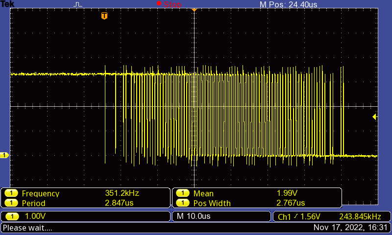
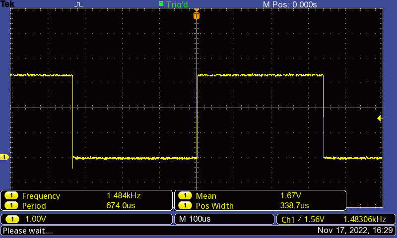
In some cases the programmable attenuation provided by the SDR can be adjusted dynamically for the best use of the available dynamic range.  In addition, there is always the possibility of digital overload and/or digital gain control via numerical scaling within the numerous digital signal processing stages of the software.  These are subjects for a different discussion.  Here, I’m talking about filters.

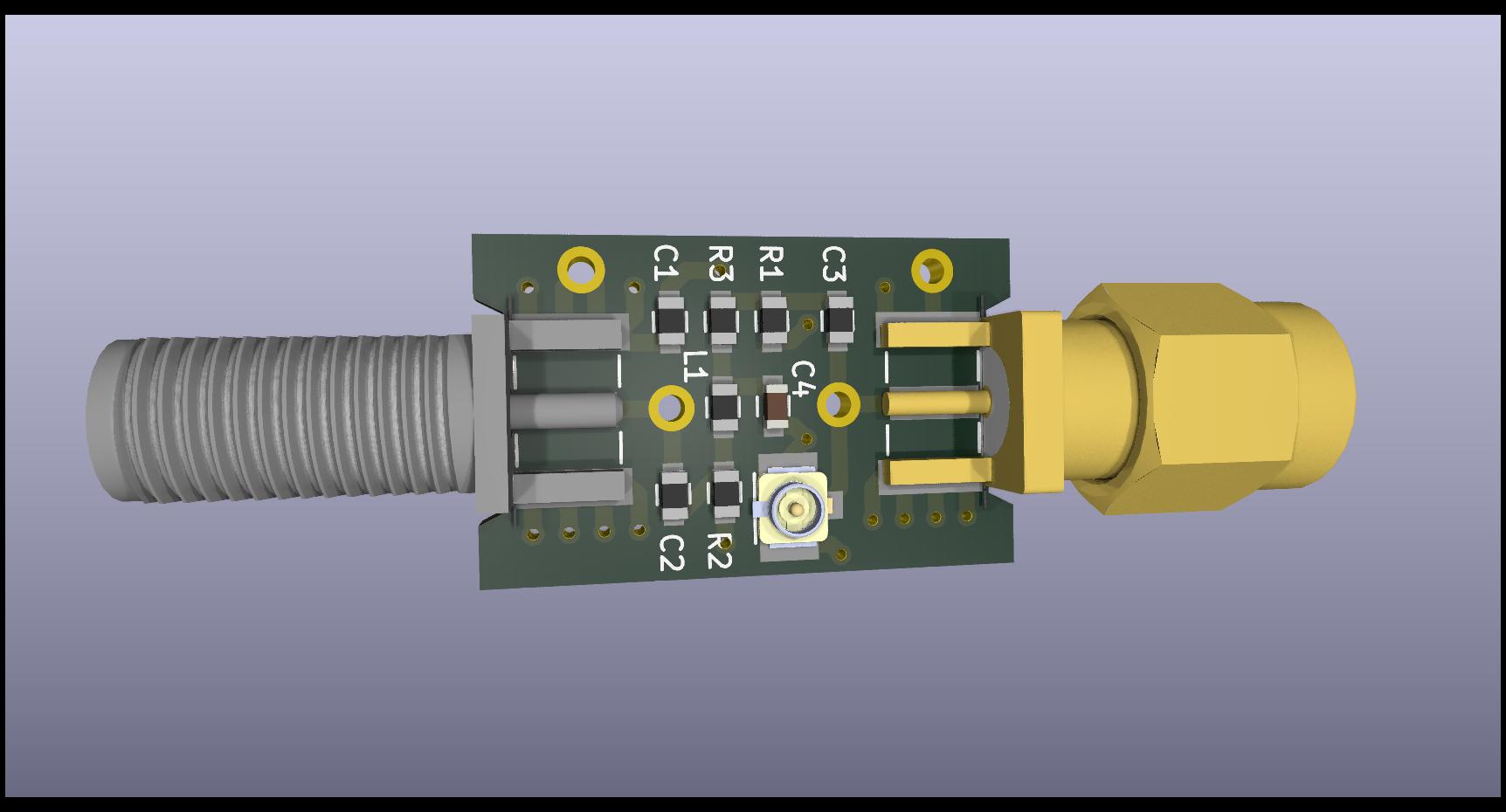
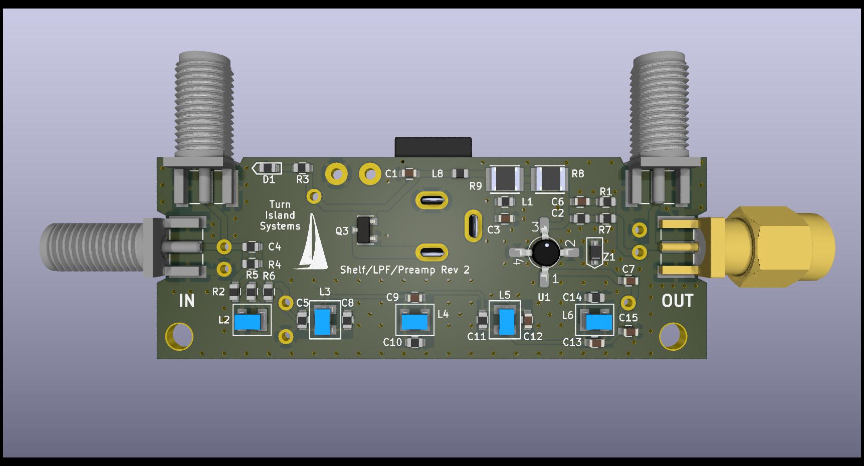
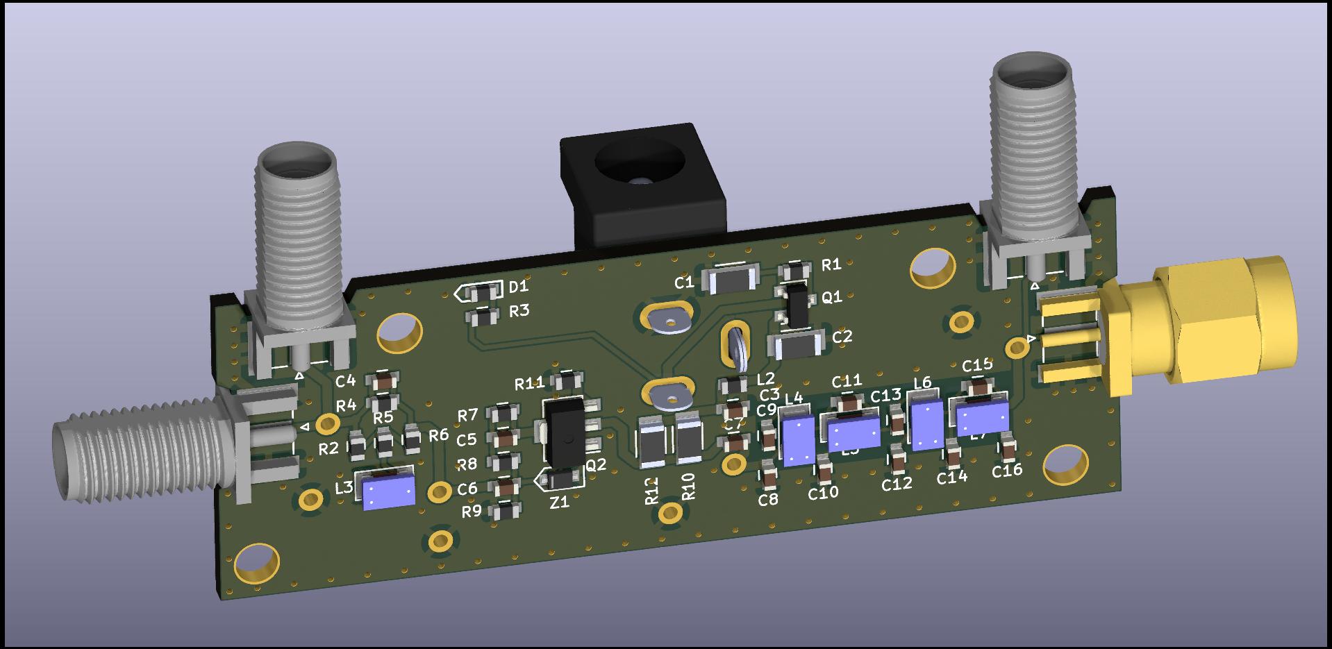
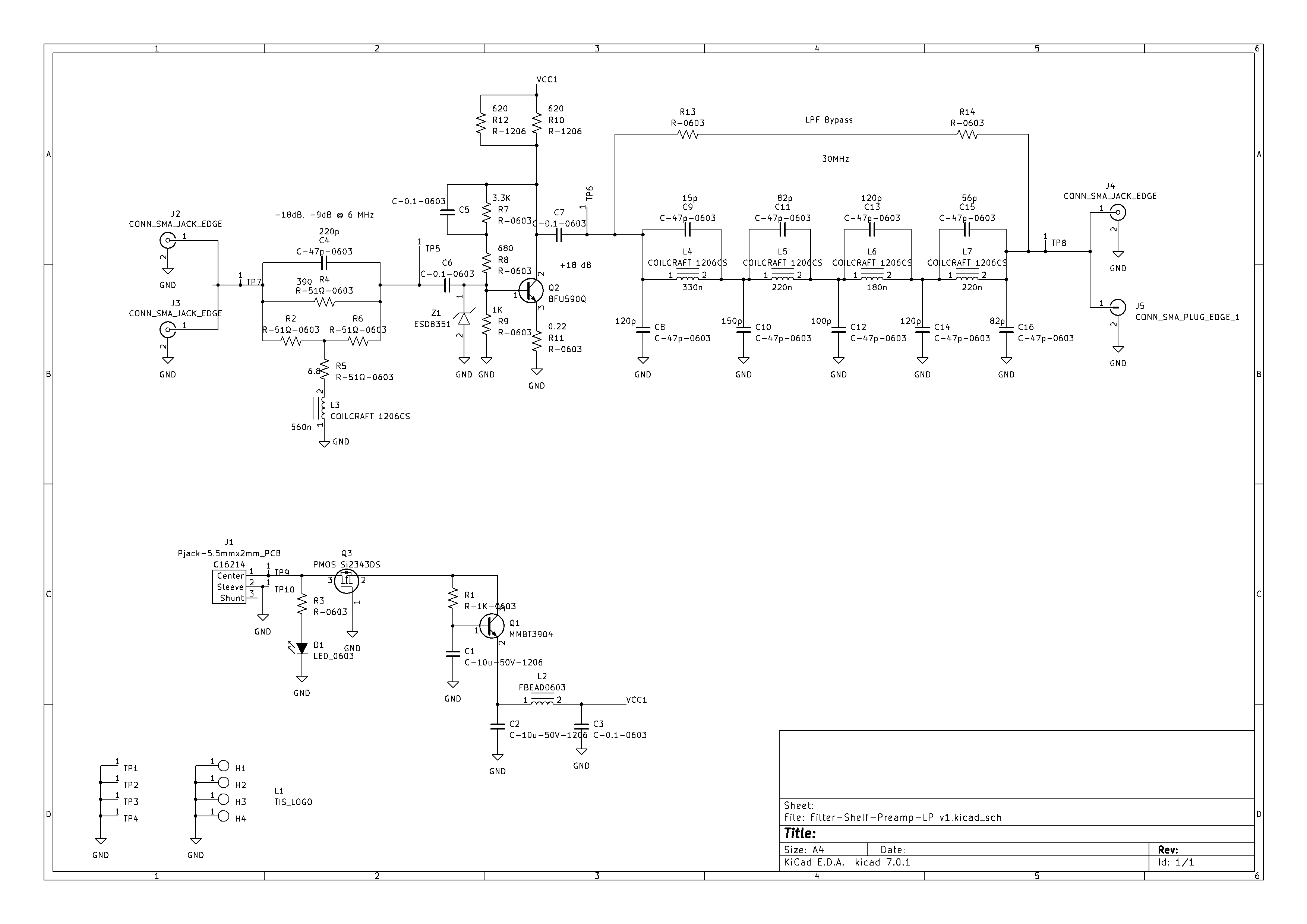
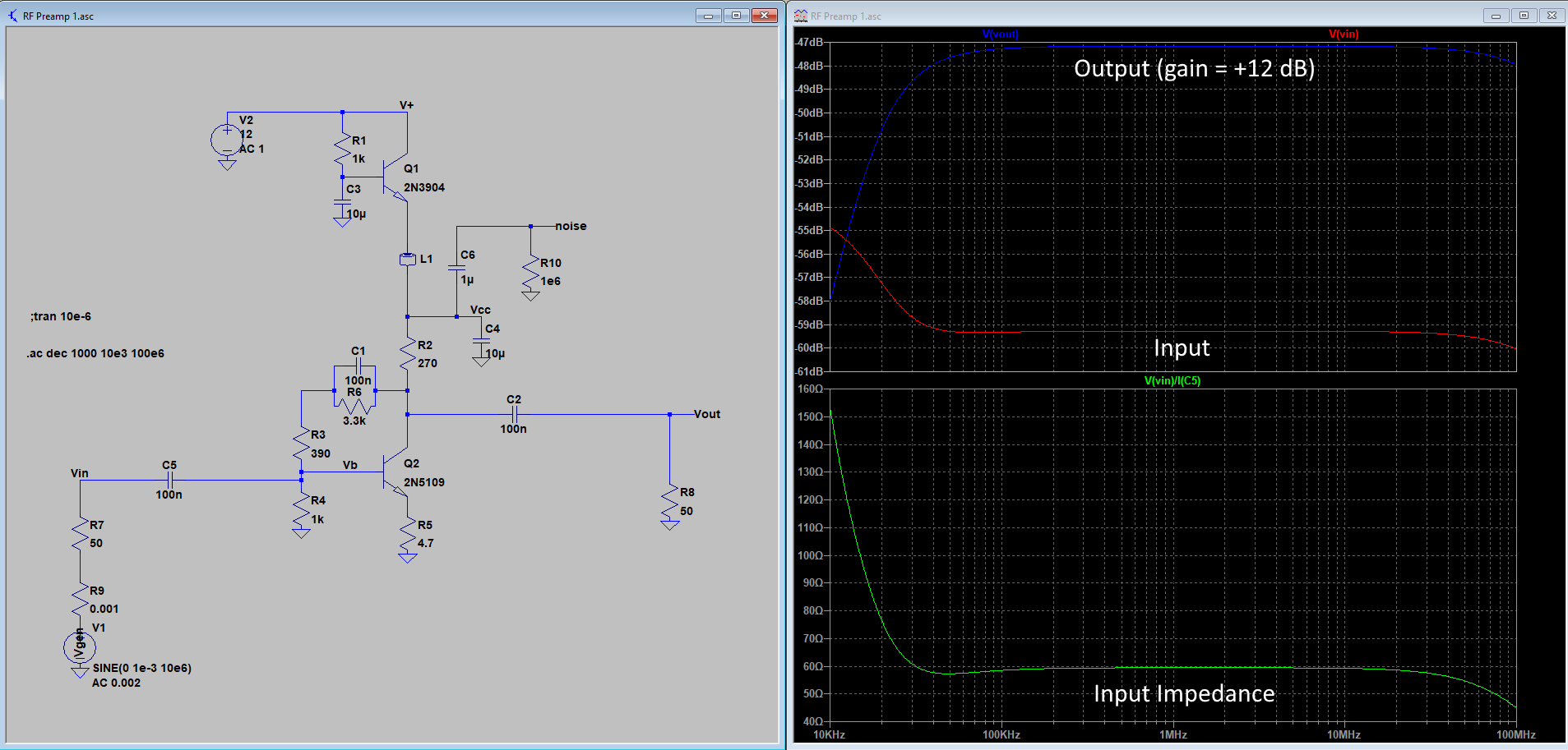
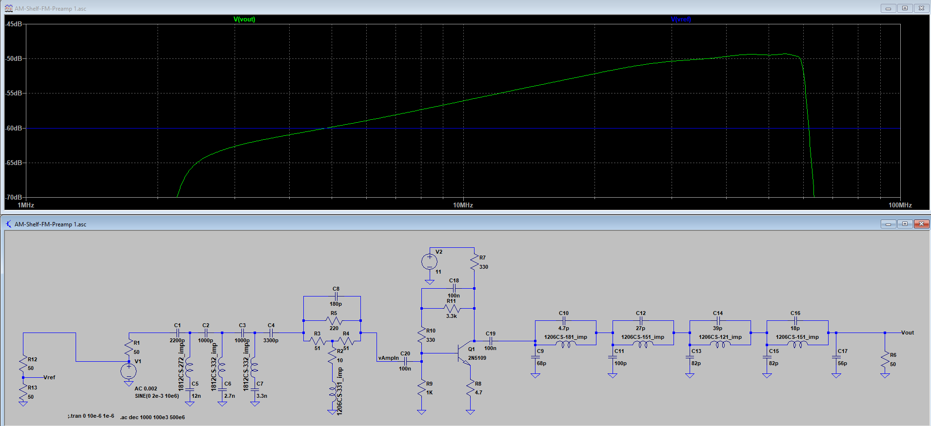
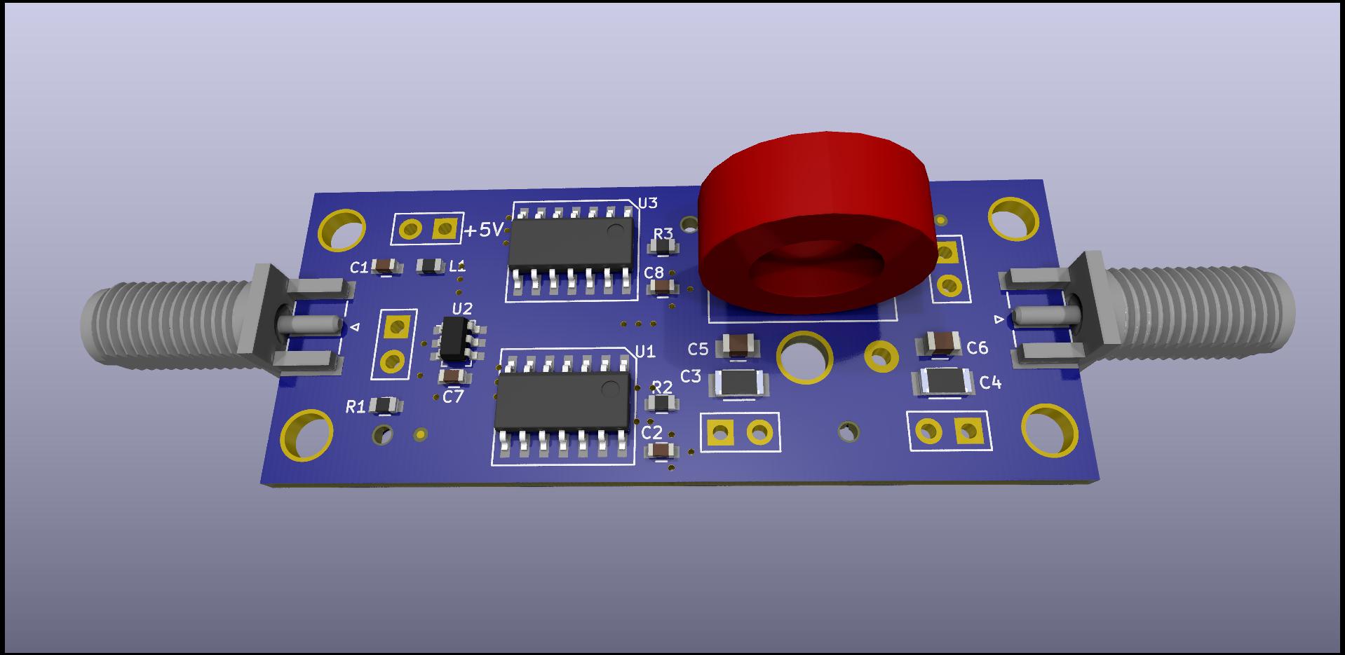
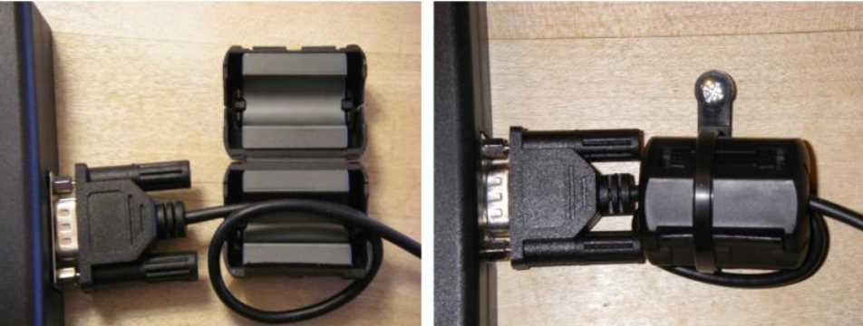
While some amount of ADC over-range clipping is tolerable, we usually try to minimize this by inserting attenuation or otherwise setting the gain before the ADC sufficient to avoid significant overloads.  We also use a moderate amount of frequency-shaped filtering to reduce input levels at lower frequencies where the general atmospheric noise establishes a higher noise floor.  The Turn Island Systems SDR Filter and Filter-Preamp are examples of this type of filtering:

Shelf filter with 30 MHz anti-alias LPF

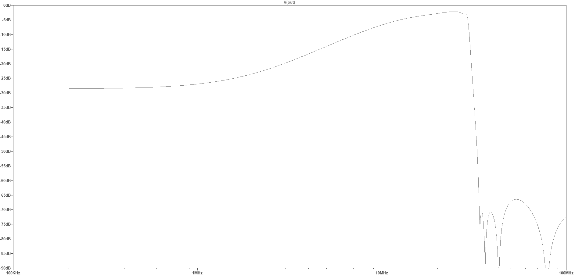
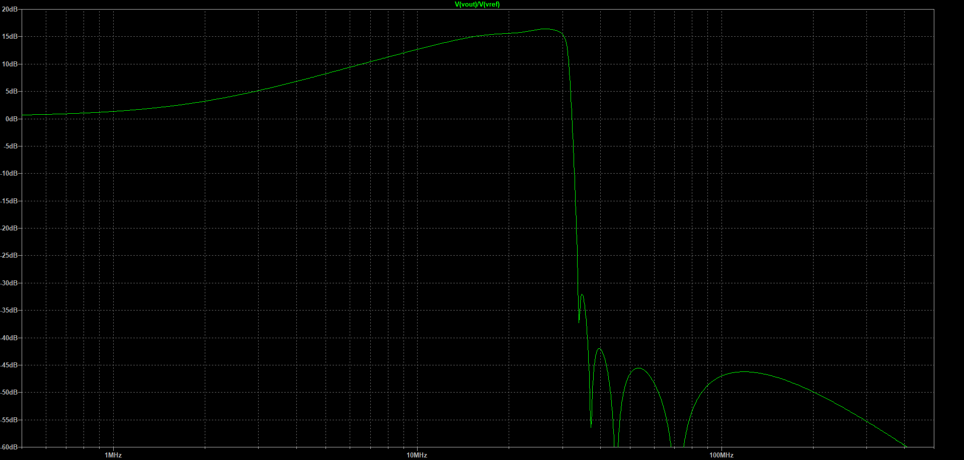
This filter has a steep 30 MHz anti-aliasing low-pass filter, and a high-pass “shelf” filter that attenuates the frequencies below around 10 MHz, flattening out below 1 MHz to a “shelf” attenuation of about 28 dB.  This shelf filter roughly compensates for the change in the general atmospheric noise level, and attenuates the USA AM BCB (broadcast band, 540 – 1700 KHz) , helping reduce the chance of ADC overload.

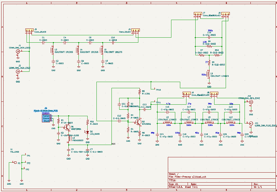
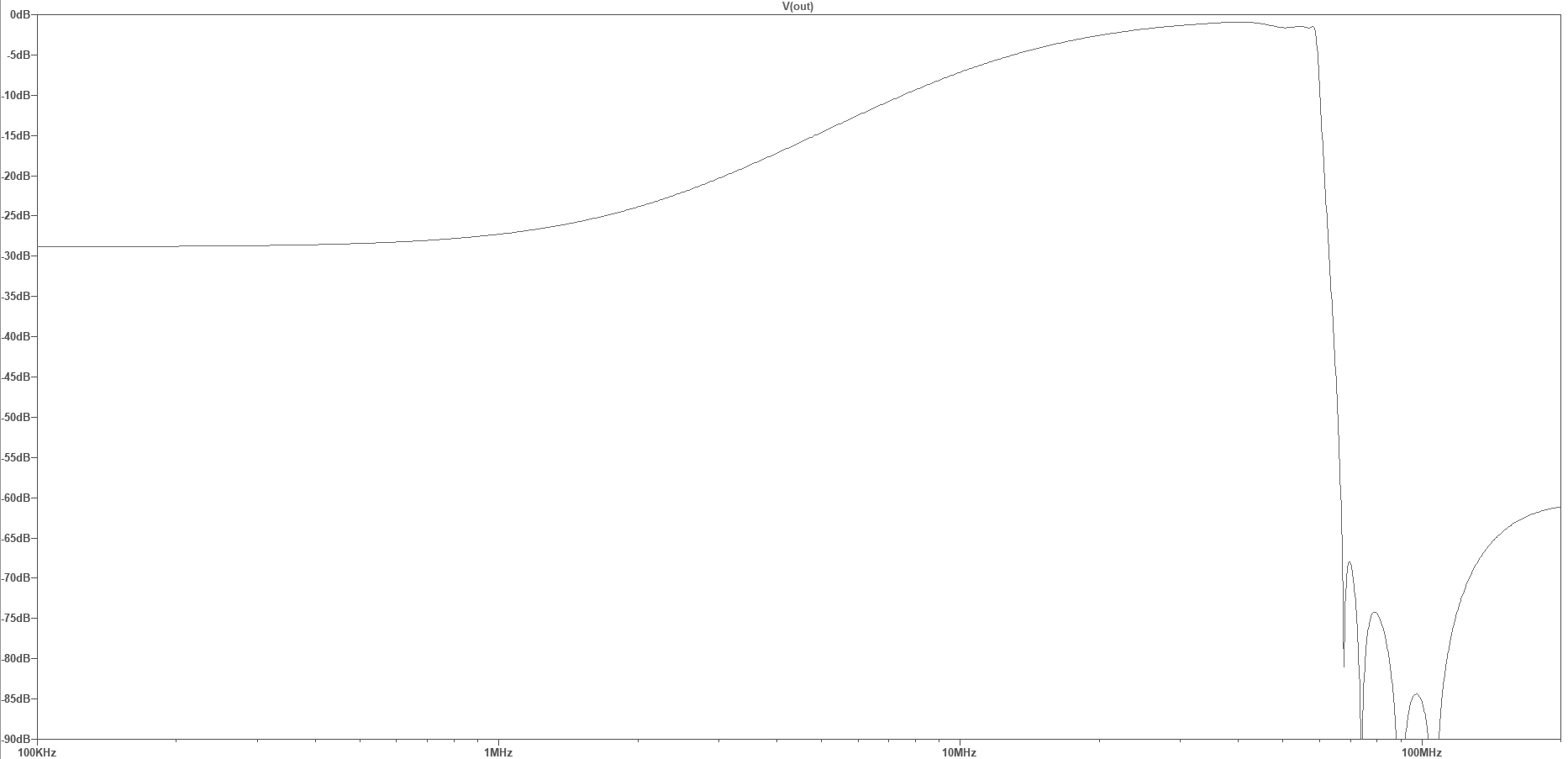
A similar filter/preamp (under development) places the LPF corner frequency at 60 MHz, allowing reception of the 6-meter ham band (requiring a RX-888 SDR sample rate of 130 MHz).  This filter also has the stopband notches placed to optimize attenuation of the 88 – 108 MHz FM broadcast band, which would otherwise be aliased down to 22 – 42 MHz in frequency.  While the RX-888 does have a built-in 60 MHz LPF, it’s characteristics are pretty marginal (see the links at the end of this post for more details).

Shelf filter with 60 MHz anti-alias LPF

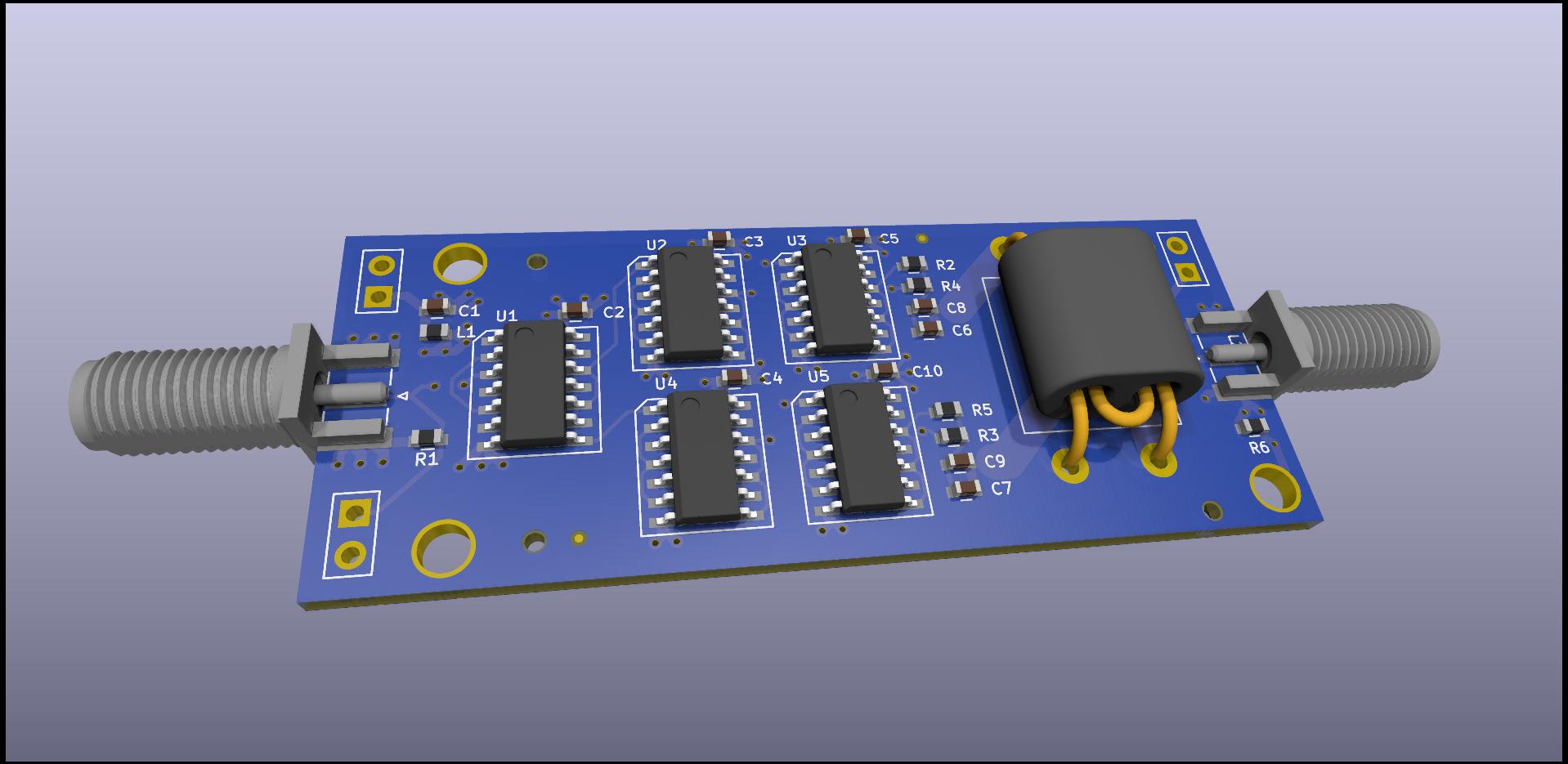
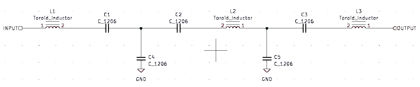
While the shelf filter reduces the chance of AM BCB overload, strong signals elsewhere can still cause problems.  If these are in the ham bands then simple filtering is not going to help.  But some people are using tunable notch-filters to attenuate specific signals, or ham-band bandpass filters to attenuate out-of-band signals.  Here is an eight-band bandpass filter I am currently working on (I’m calling it the BPF8):

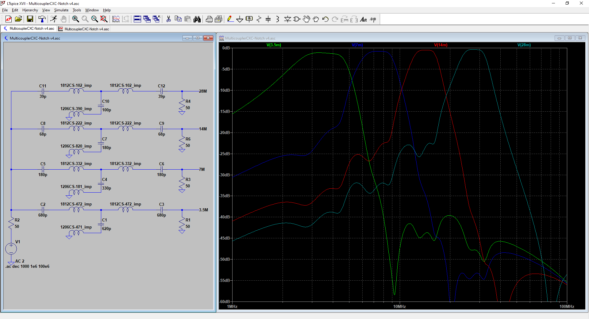
The BPF8 is actually a bank of three-section bandpass filters connected in parallel.  Each filter has this design:

One of the eight band-pass filters

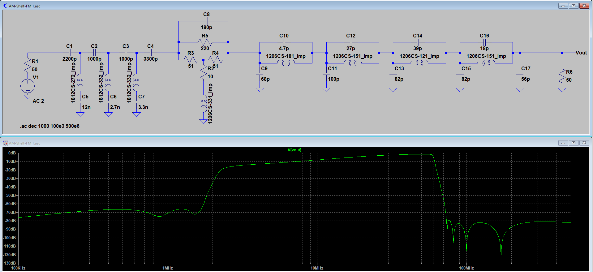
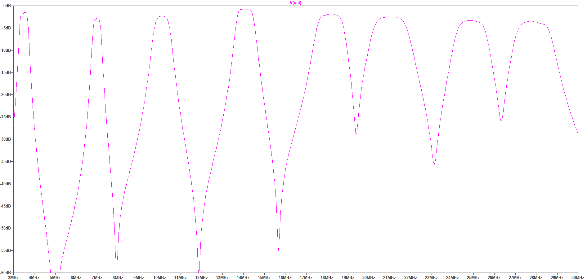
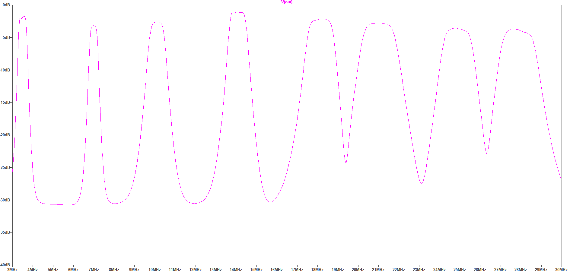
The (simulated) overall response looks like this, covering the 80, 40, 30, 20, 18, 15, 12, and 10 meter ham bands.  These filters are tuned for the WSPR sub-bands:

BPF8 frequency response (linear frequency plot)

Will this help with SDR dynamic range?  That depends on the interference — if the out of band signals aren’t strong enough to create problems then this filter will be unnecessary.

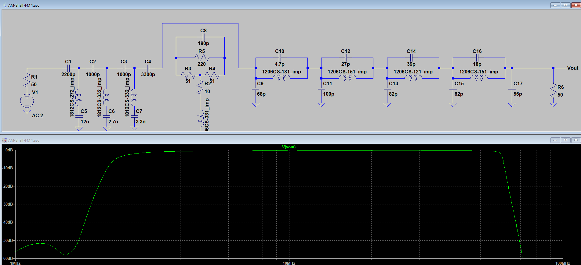
If reception between the filter bands is still desired, a broadband shelf response can be selected (via a jumper), which limits the maximum attenuation — here, to 30 dB:

BPF8 frequency response, -30dB shelf (linear frequency plot)

In the USA, most of the BCB signals are below that 1700 KHz frequency. But in Europe there are many powerful broadcast transmitters scattered over the HF frequencies, and these can cause big dynamic range problems.  Here are the shortwave BCB frequency bands superimposed on the above multiband filter response (some of these bands are only lightly or regionally in use):

Shortwave broadcast bands

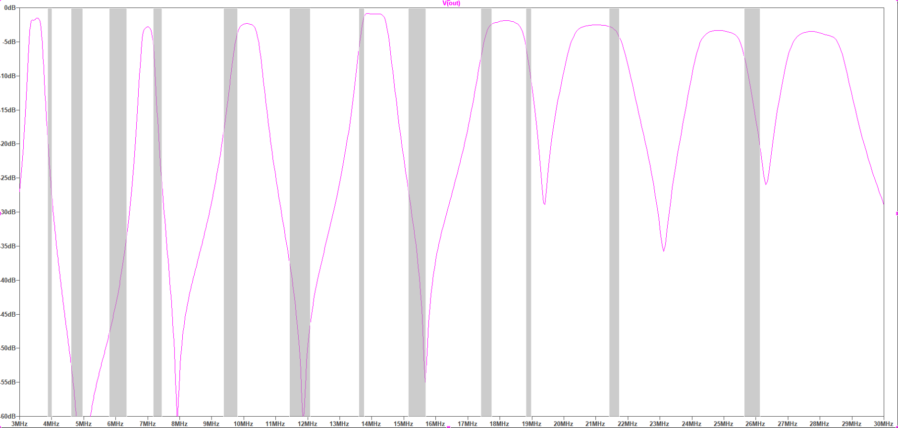
As you can see, some of these SW BCB frequencies are extremely close to the ham bands, and so in those cases the filter will probably not help much, while other SW BCB signals will be significantly attenuated.  The  BPF8 will probably include jumper options to optionally disable a selected filter section. Is the BPF8 worth a try?  We shall see.

BPF8 circuit board
BPF8 circuit board

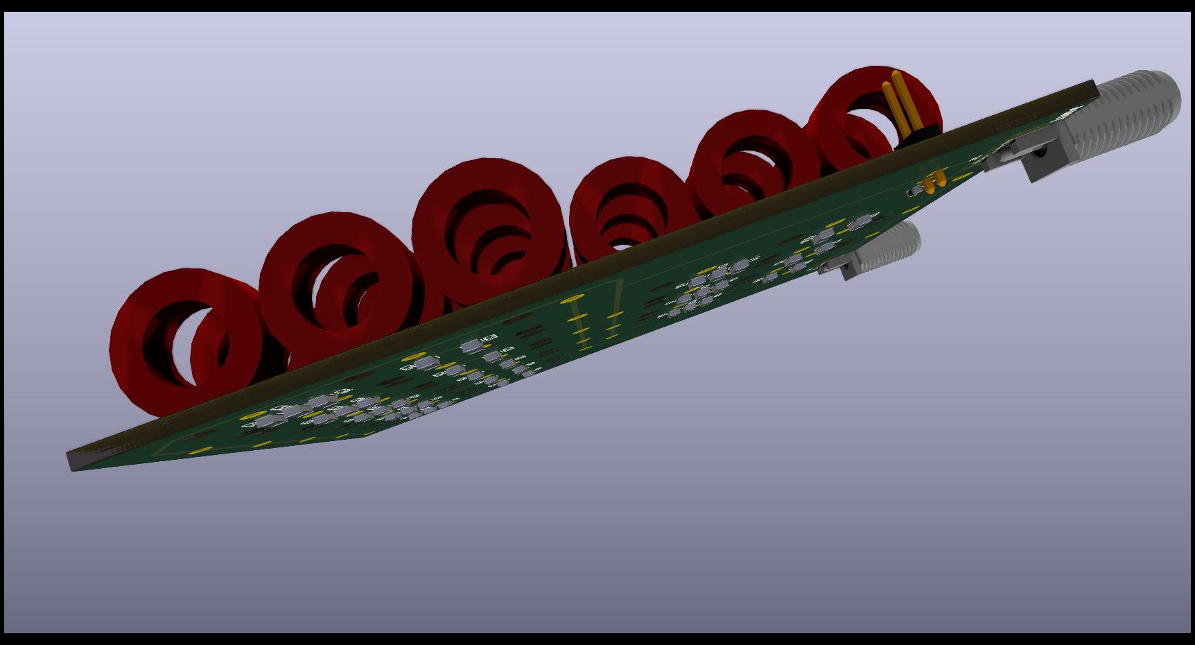
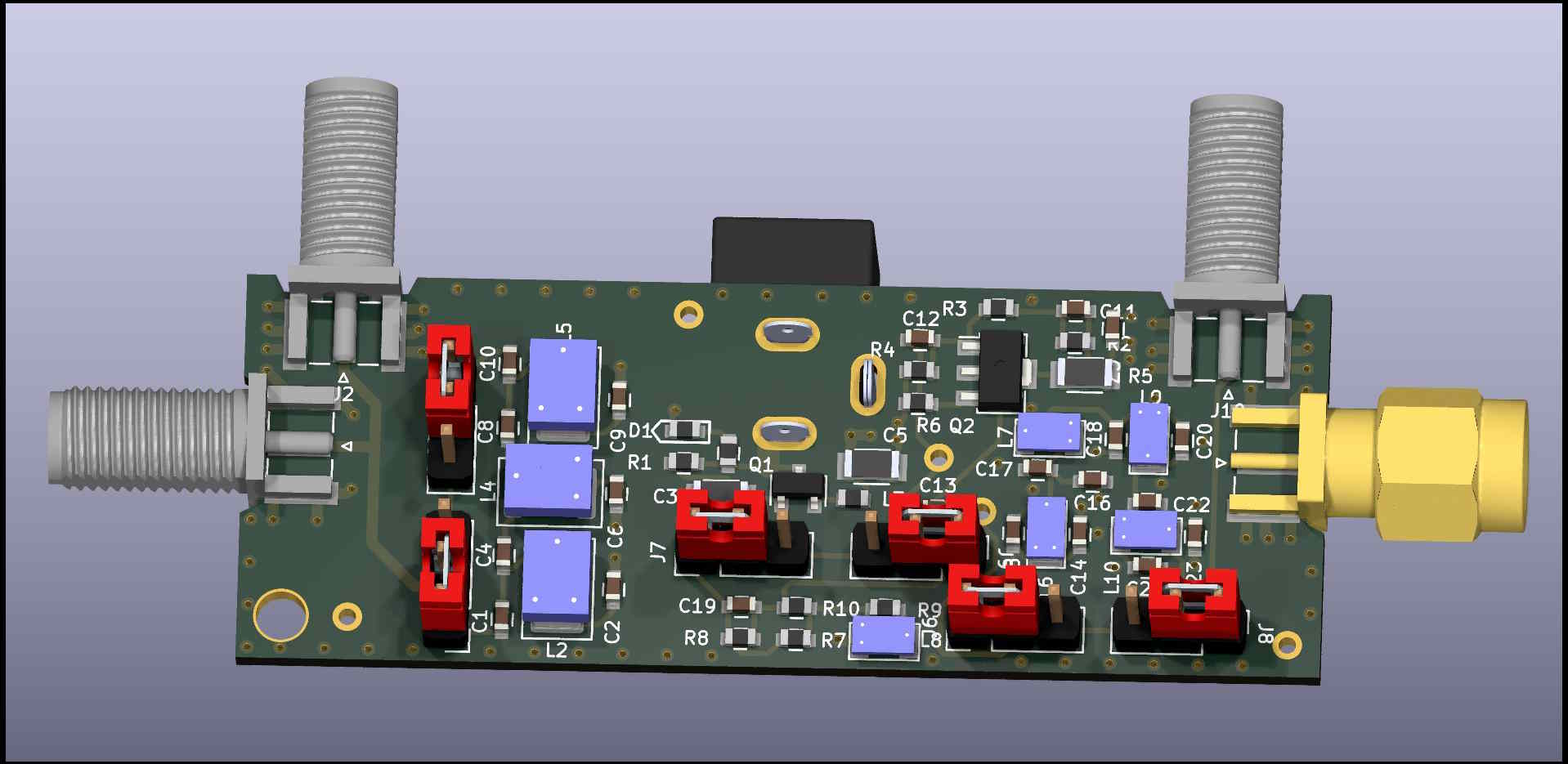
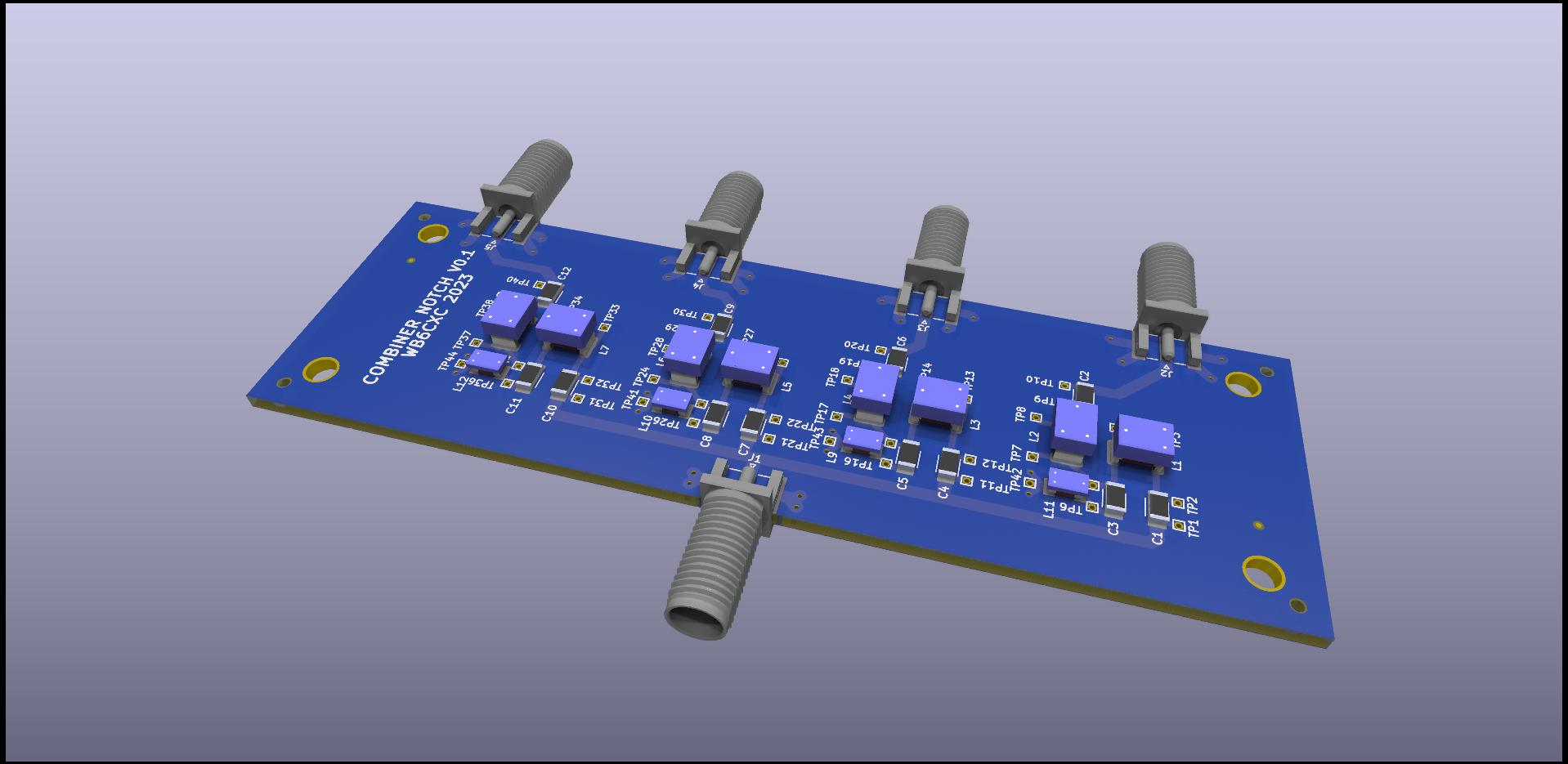
The BPF8 prototype board is densely populated with 24 toroid core inductors, used for their low-loss and self-shielding characteristics.  The filter capacitors are on the underside of the board.  This will be another “hard to build” design, because of all the hand-wound and tuned toroids, but I hope the results will be worth it.

For more details of the RX-888, and about shelf filters, look at KA7OEI’s blog for some excellent in-depth discussion of these issues:

measuring-signal-dynamics-of-rx-888-mk2

frequency-response-of-rx-888

revisiting-limited-attenuation-high-pass-filter

International broadcast bands:

International_broadcast_bands (Wikipedia)


A Whole Bunch Of New Designs

I’ve been busy.  Here is the latest batch of designs that have been sent out for fab.  Some are simple, some more complicated, and some are updates of earlier designs.  KiCad and JLCPCB sure make this stuff easy!

Look for these designs to show up on the Turn Island Systems website.

RX-888 External Clock Interface Kit:

RX888 Ext Clk 1 front


BackPanel v1 front

This is a fairly simple kit that provides termination, appropriate attenuation, and DC isolation for the external clock interface to the RX888 SDR.  This includes the interface card, and a replacement back-panel for the RX888.  The complete kit will also include a short U.FL jumper cable and a piece of thermal foam gasket that is used to reduce the RX888 internal temperature rise.

That SMA plug shown on the right side of the board is not present when this board is installed inside the RX888, but can be soldered on when the board is used externally.

Updated Clock Distribution Buffer:

Clock Dist v2.0 cropped

The existing five-output clock buffer has proven quite useful for distributing reference clocks in multiple-SDR receiver systems.  Since I am running out of that unit, I have sent this upgraded design for fabrication and assembly.  This new design now provides six outputs, each with jumper-selectable AC/DC coupling on both the signal and ground connections.  The AC coupling won’t make any difference if you have RF ground-loop issues, but can really help with DC/power supply ground issues (as we often see with USB-powered devices).  This new board also provides a power/clock indicator LED.

AC-Coupled SMA Adaptor:

Isolator 1 top

This tiny board provides capacitor-coupling for both signal and ground.  While it’s simple, it can be very useful when dealing with grounding issues.  Note that the commonly-available DC-block adaptors only block the signal pin, and still leave the grounds connected.

Filter/Preamp V2:

Filter-Preamp v4

This is my second try with the filter-preamp.  I have rearranged the low-pass filter to (I hope) reduce blow-by, and have upgraded the amplifier to use a Minicircuits MAV-11BSM+ device.  This should improve the intermodulation distortion and provide a good noise figure.  I have also moved the amplifier to the output of the low-pass filter, to reduce potential out-of-band overload issues.

The SMA jack and plug positions provide the option for the in-line jack/plug and right-angle jack/jack configurations.

I may eventually replace the MAV-11 amplifier with a high-speed current-feedback amplifier, which should result in excellent distortion numbers,  reasonable noise figure, and lower power consumption.  But for now the current design should be a good performer, and I want to verify the performance of the new filter arrangement.

Swiss Army Knife vs Can Opener?

In my last entry I described a feature and option-laden filter/preamp board, comparing it to a Swiss Army Knife.  Great, but sometimes you just want a can opener…

After some serious discussion about how such a design would be used, and the typical requirements, I’ve decided that a major simplification is in order.  (And, of course, a new feature)

Filter-Preamp-simple v1

The consensus was that there was no need for bypassable filters, so the stages are now:

  • 18 dB shelf filter (-9 dB @ 6 MHz)
  • 17 dB preamp
  • 30 MHz elliptic low-pass filter (or 60 MHz as a different assembly)

This board is powered by an external +12V DC supply, and draws about 20 mA.  There is an active-filter stage that should clean up most supply noise.  The new feature is simple low-loss reverse-polarity protection for the power input.

Here is the (simulated) gain of this unit:

simpleAnd the schematic:

Simple Schematic

Actually, the two filters can be bypassed at assembly time as a load-option.  Perhaps this will let this board also be used as an amplifier-only design.

I have sent this design out for PCB fabrication and ordered the components — I can’t wait to see how it all comes together!


A Combined Multi-Section Filter and Preamp

Many SDR receivers, especially those designed for full HF-spectrum use, have needed various filters and preamps between the antenna and the SDR.  High-power AM and FM broadcast stations can overload the receiver front-end, so these are filtered out.  The characteristics of atmospheric background noise are such that a “shelf” (or “shelving”) filter which attenuates the lower-frequency range can also be useful in optimizing the SDR dynamic range.

Finally, the SDR sensitivity / input noise-floor at  the higher end of the spectrum can be marginal.  Add the inherent losses of all these filters and a low-noise, high dynamic-range preamp becomes very useful.

So I am designing the “Swiss Army Knife” of SDR front-end modules:Filter-Preamp

No, there aren’t four SMA connectors, only one pair will be installed, giving an “in-line” version, and a “right-angle” version that can fit on a small die-cast enclosure.  There are four sections to this board:

  • AM Broadcast Band filter
  • 15dB Shelf filter
  • 13db gain preamplifier
  • FM Broadcast Band filter

Each of the filters can be bypassed using pin headers and jumpers.  The amplifier components can be omitted during assembly and a jumper used to bypass this section.

The FM band filter allows for 6-meter reception, but many SDR receivers are clocked at 66 MHz or so, and require a lower corner frequency on the low-pass filter.  This filter can optionally be built with a corner frequency at 30 MHz.

Amplifier:

Amplifier

Amplifier simulated with 2N5109

The amplifier is a simple wide-band zero-inductor design (found in the November 1984 edition of Ham Radio magazine, page 100: https://www.worldradiohistory.com/Archive-DX/Ham%20Radio/80s/Ham-Radio-198411.pdf).  It’s become difficult to find the classic 2N5109 transistor, so I am using the more modern BFU90Q, which has similar performance.  But I am simulating with the 2N5109 because that’s the model I could find.

The amplifier draws about 20 mA from a +12V power source, and my board includes a simple but effective filter that eliminates most noise and ripple on the DC source.

Here are the three filter sections:

filters 1

From left to right the first filter is the AM broadcast filter,.  This starts attenuating below 3 MHz, and is at least -50dB down at the top of the AM band.

Next is the 15 dB shelving filter.  In a previous filter I had two 10 dB shelf filters in series, with each of them bypassable.  This limited-size board requires a compromise, so there is just a single filter section.  The inclusion of the AM BCB filter should mitigate the effects of the simpler shelf filter configuration.

The right-hand filter is a elliptic low-pass design, that cuts off at 60 MHz.  The  attenuation in the FM broadcast band, and above, is approximately 80 dB.  This is also an excellent anti-aliasing filter for the SDR.

With the shelf filter bypassed the filter response from 3 to 60 MHz is essentially flat:

filters 3

With all filters and amplifier enabled, the overall gain at 60 MHz is about +10 dB.  The input (blue trace) is -60 dBm, and the output (green trace) is -50dBm :

filters+amp 1

And here is the schematic for the whole thing:

SchematicThe simulated performance shown above should be reasonably close to the actual thing.  At these frequencies the inductors are the largest source of simulation errors, but I am using Coilcraft inductors and their provided simulation models.  These have proven to be remarkably accurate in previous designs.

But this is a tight little board, and layout parasitics may be an issue.  You will see that the (unshielded solenoid) inductors have been oriented to reduce coupling, and (which you can’t see) the ground planes have been relieved underneath the most sensitive tuned circuits.  I do hope that the amplifier won’t turn into an oscillator, but the design and layout do give me some optimism.  I plan to have a working prototype in about a month.

Like the Swiss Army Knife, this design may not be the best tool for every job, but it should be useful in SDR receiver systems.

Acknowledgement: I would like to thank Clint Turner / KA7OEI for his invaluable advice on filters, amplifiers, and optimizing SDR performance.  His excellent blog: https://ka7oei.blogspot.com/2020/08/revisiting-limited-attenuation-high.html


Latest Batch of Boards

I’ve just received another batch of QDX External Reference Interface boards.  More info at Turn Island Systems

Also, I just sent out boards for a four-channel RF Combiner / Splitter, which takes four 1W (or lower) signals (80, 40, 20, and 10 meters), and combined them into a single output for feeding a multiband antenna.  These provide at least 20dB port-port isolation, and less than 2dB loss.  If all works as planned, these will be used for Ionospheric research.

MC-CXC-Notch

RF Combiner Notch v0.1 top

And finally, here’s a 1W (approximately) power amplifier, using 74ACT04 digital integrated circuits to drive a wideband transformer.  This takes a 3.3V digital input between 3 and 30 MHz, and produces a 1W square wave output.  External filtering will be required, and the combiner shown above should provide adequate filtering.

OneWATT v0.1 top

There are “better” ways to make a 1W amplifier, but this is quick and easy, and requires no tuned circuits.  I can’t wait to test these designs!

A Little Amplifier

QWATT 0.2 top

In the process of turning my three-output Si5351-based “ClockBox” into a three-band simultaneous FST4W beacon, I decided I needed a small power amplifier to boost the (approximately) 10dBm square-wave outputs up to a 1/4-watt clean sinewave.  Rather than using FETs and transformers, or a Class-E design, I decided to try using the an 74ACT04 hex inverter as the power stage.  Each inverter output can deliver in excess of 25 mA  with about a 4.2V swing (+5V supply) so six of them in parallel looked promising.  And I happened to have a full tube of old 74ACT04 parts in DIP form (remember those?)

So I built one, tuned for the 15 meter ham band:

breadboard 1(Ignore those power-level numbers, I had a bad coax jumper)

I was worried about connecting the outputs directly, afraid that skew would result in excess output-stage current, but some tests showed low unloaded dissipation  up past 30 MHz.  Adding small resistors at each output might be a good tradeoff, but for now I decided not to waste the power.

I used a simple L/C impedance-matching network to transform the 50 Ohm load (antenna) down to about 3 Ohms which matched the ganged inverter output impedance.  Instead of a simple series inductor I used a series L/C, calculated to provide the correct reactance at the design frequency, but giving a high impedance at higher or lower frequencies, and a bit of extra filtering.  This also makes the design slightly more bulletproof — you can run any frequency into it without causing excess dissipation.

The output power of the test board was actually closer to 1/2 W, and the harmonics were slightly better than 40 dB below the carrier.

PNG2


The amplifier efficiency is about 60% and the temperature rise on the buffer was well within comfortable limits.  This is good enough that I am having some circuit boards made.  The only frequency-sensitive components are two capacitors, and one toroid inductor.  I would have liked to use small surface-mount inductors, and the board does provide for that option, but the toroid has much lower loss.  The board uses two surface-mount 74ACT04 parts, and a small buffer to drive the 12 inverter inputs.