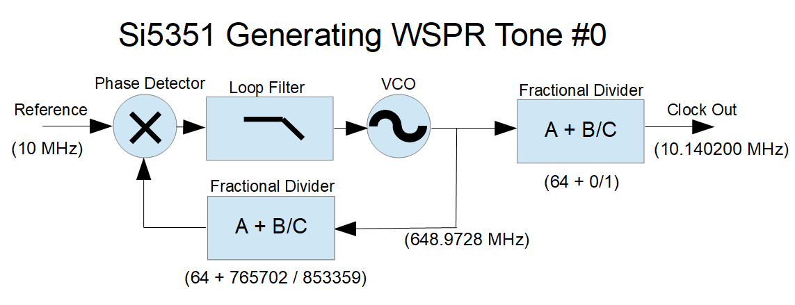
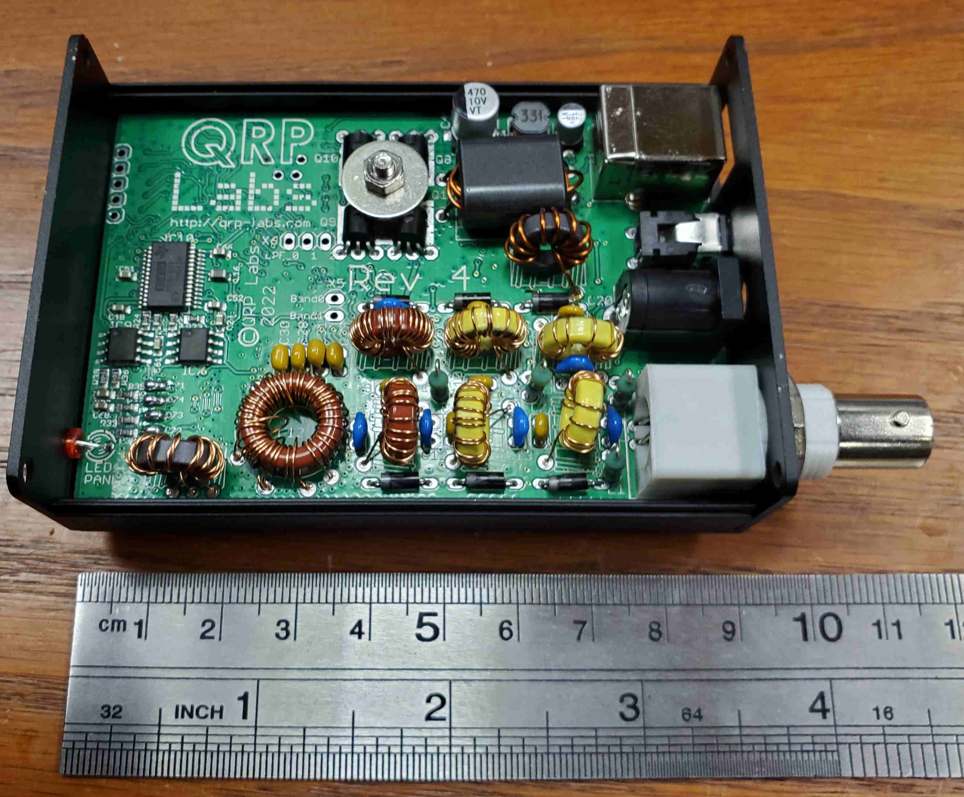
I recently built the QRP Labs QDX transceiver, which is a remarkable little radio, designed for FSK modes (FT8, JS8, WSPR, etc.) on the 80-20 meter ham bands.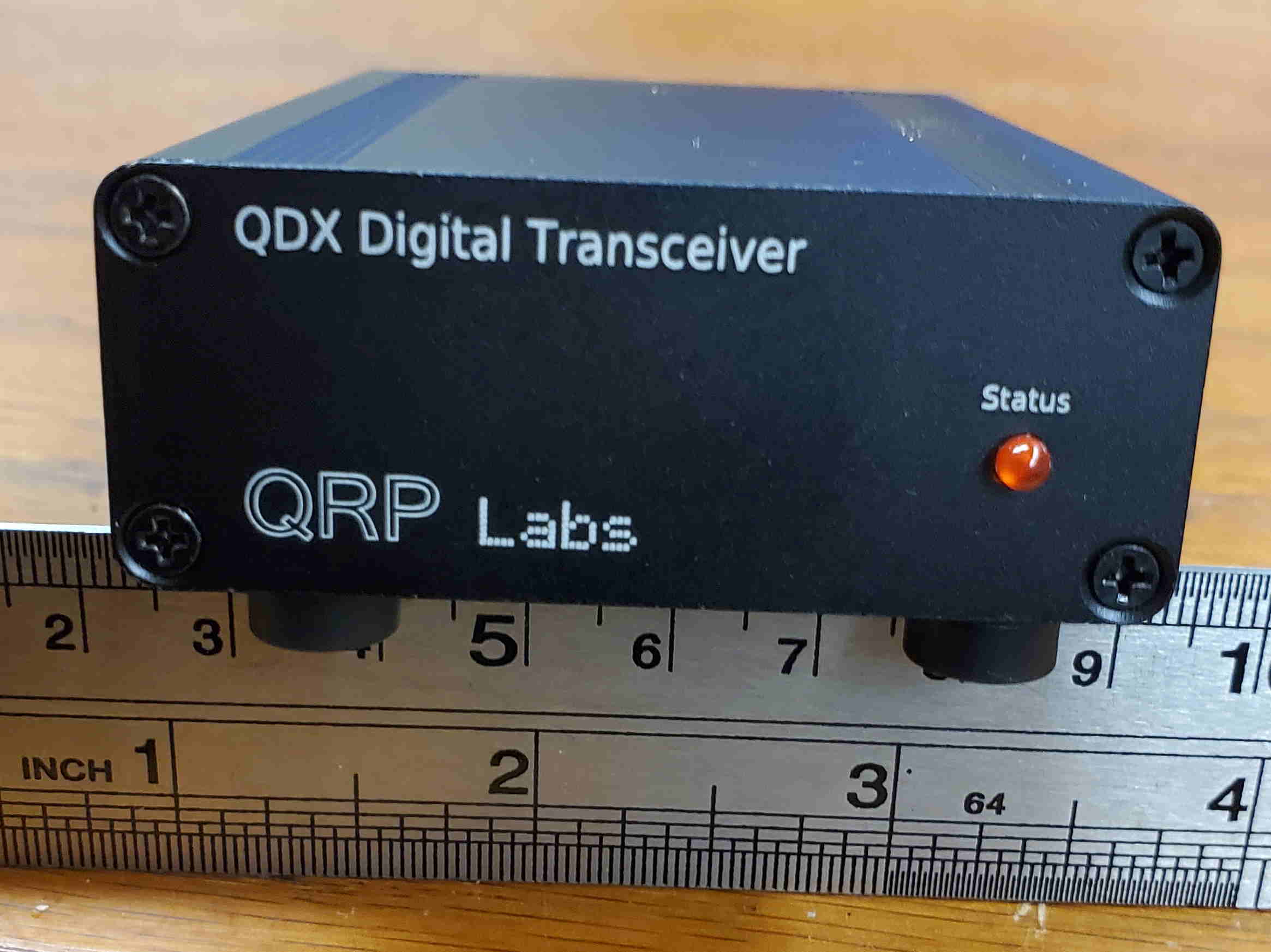 This rig has some very clever design inside. Instead of the standard SSB modulator and demodulator, this uses a USB interface for audio and CAT rig control (emulating a Kenwood TS-440), and measures the audio input tone, using that measured audio frequency and the set “carrier” frequency to program the internal Si5351 clock chip. This way it directly generates the transmit frequency — no sideband modulator / filter, no linear amplifier, just the synthesizer and an efficient Class-D 5W power amplifier.
On receive, the radio uses a “Tayloe” mixer, using the Si5351 to generate the necessary quadrature clocks. The I and Q mixer outputs are digitized and processed in a software SSB demodulator. This digital audio is sent out the USB interface, to a program such as WSJTX.
There’s much worth studying in this design and Hans Summers (the designer) has provided some excellent documentation:
https://www.qrp-labs.com/qdx.html
It took me about three hours to build this radio. The kit comes with all the surface-mount components already loaded, so I only had to solder a handful of capacitors and wind some toroids.
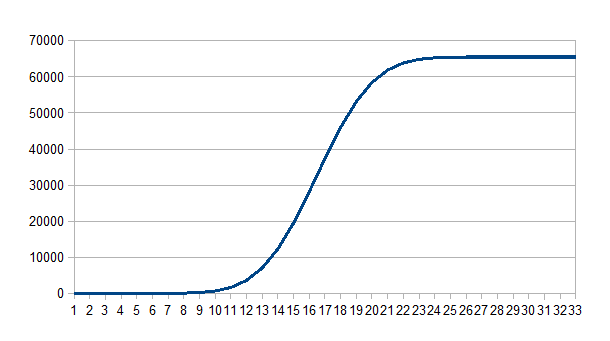
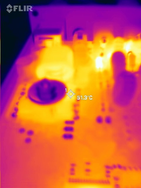
There has been some discussion about the four power transistors — they do run a bit warm and people have burned them out trying for higher power (or due to bad SWR). I ran the transmitter into a dummy load for about two minutes and measured the transistor temperatures. This had stabilized at about 50 degrees C:
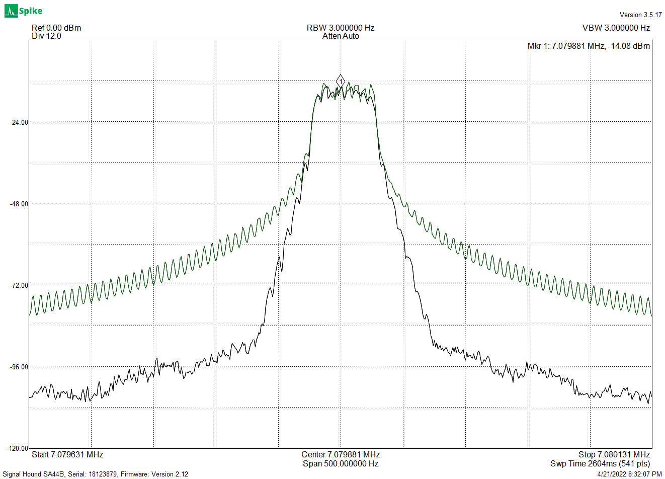
The signal transmitted by this radio is clean, with harmonics well under the FCC requirements (those close-in spurs may not actually be there. The spectrum analyzer I was using has some spurious responses of its own):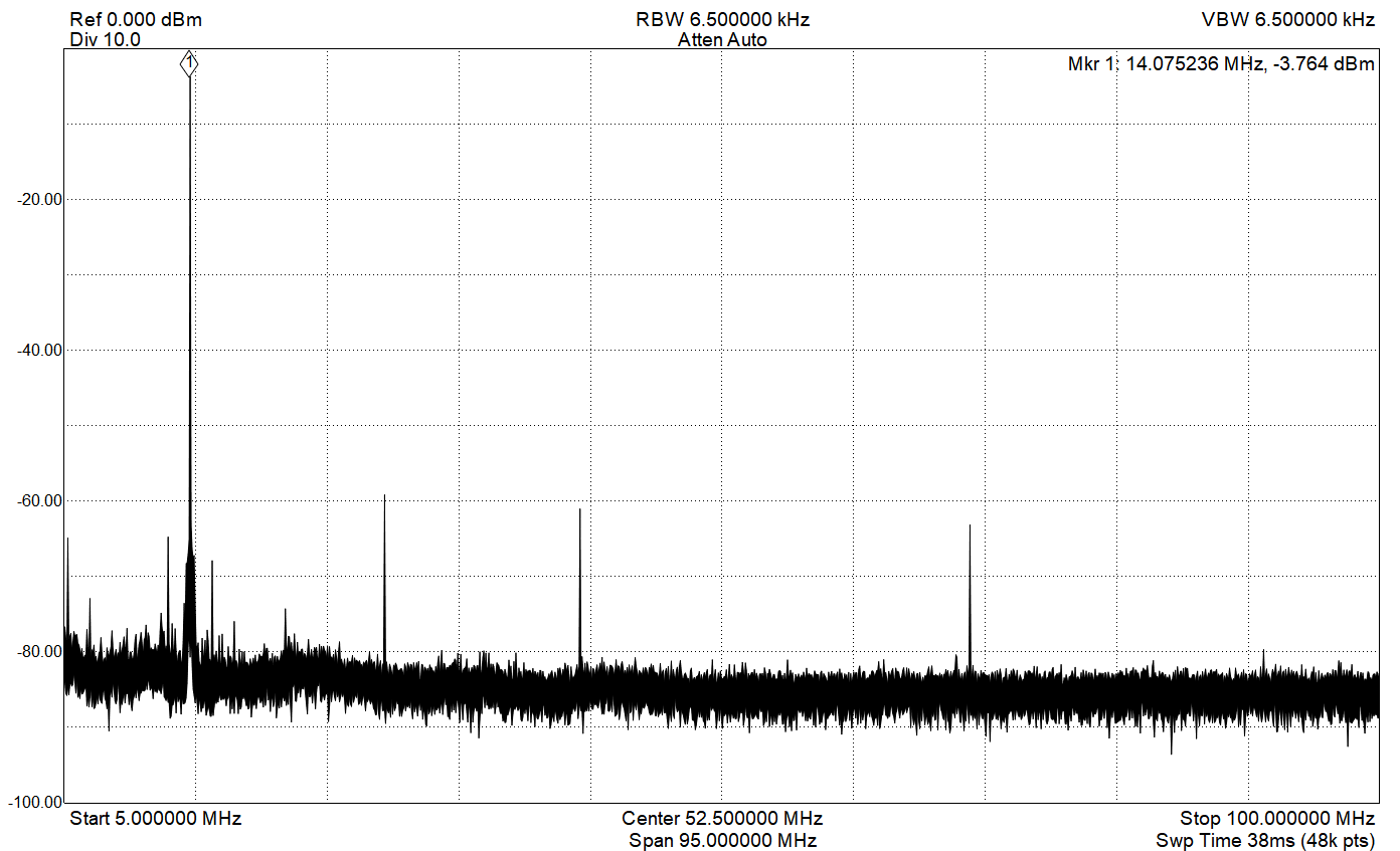
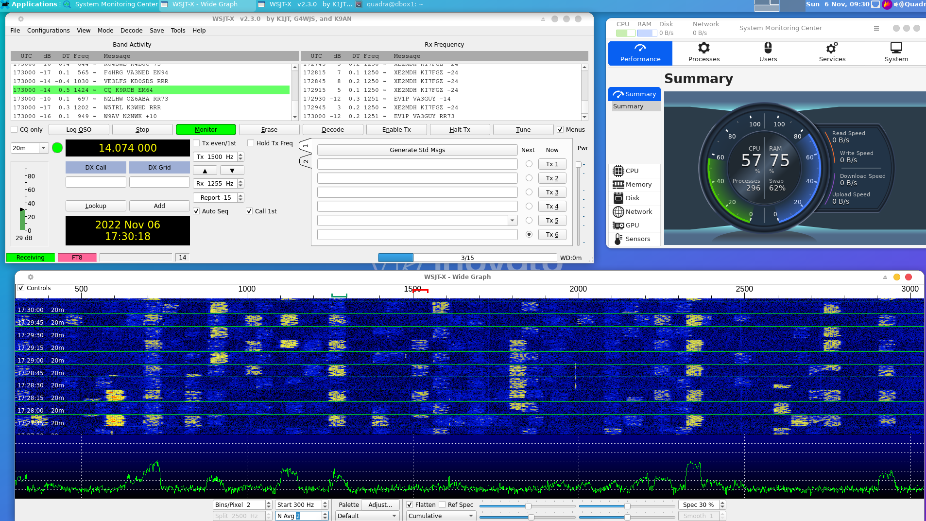
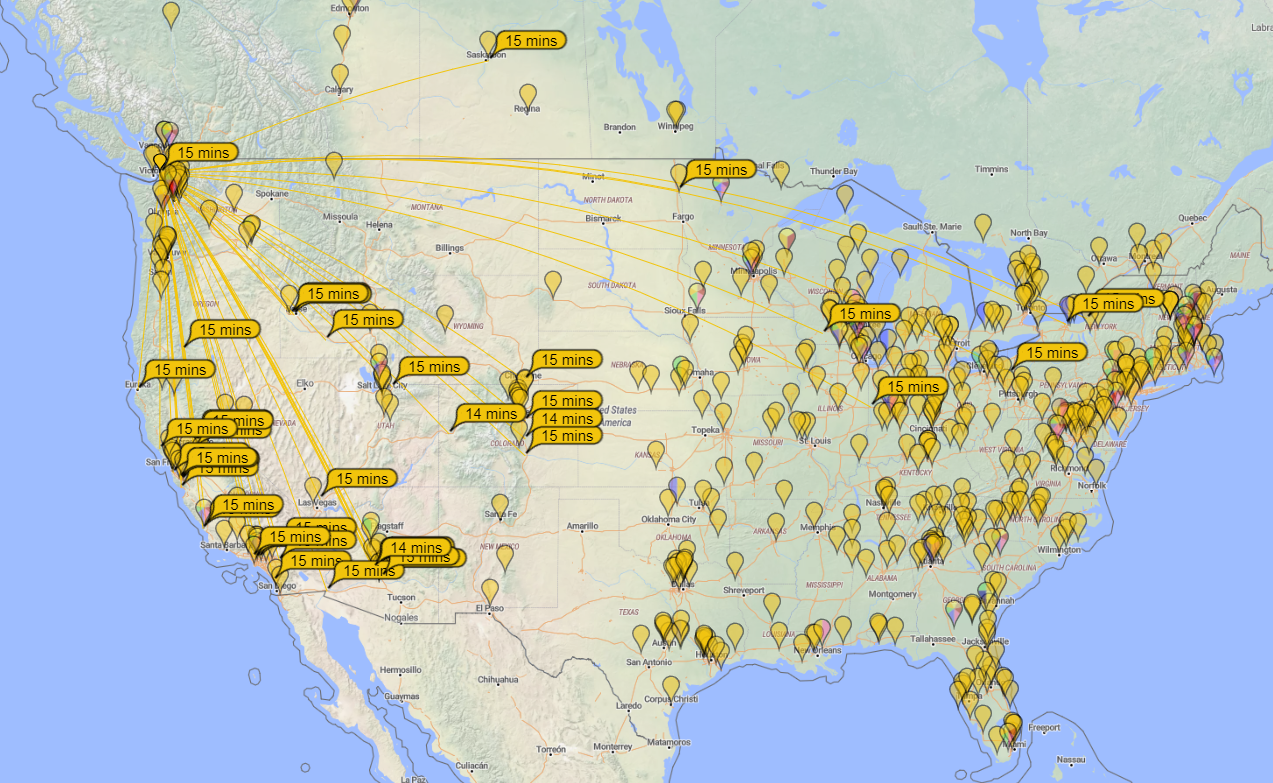
After this I gave the radio a spin on 20 meters, using WSJTX running on a small, inexpensive linux box, the Inovato “QUADRA”. This little computer is comparable to the Raspberry Pi-3, and only costs $30 (power supply and HDMI cable included). I installed JS8CALL, WSJTX, and Direwolf using the command-line “sudo apt-get install [program name]“, and everything went without a hitch. Running FT8 for a few minutes resulted in this:
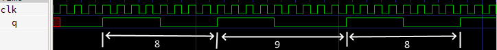
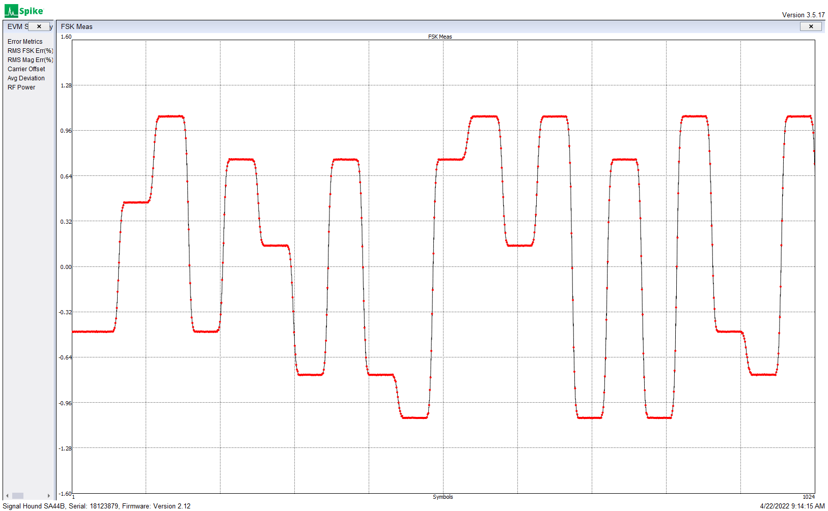
A friend had noted that the QDX wasn’t perfectly generating some of the smaller frequency shifts used in some FSK modes. Hans has acknowledged the problem and is working on a firmware update, but I decided to look into this. First I used my “Signalhound USB-SA44B” spectrum analyzer, in the modulation analysis mode. FT8 looked good:
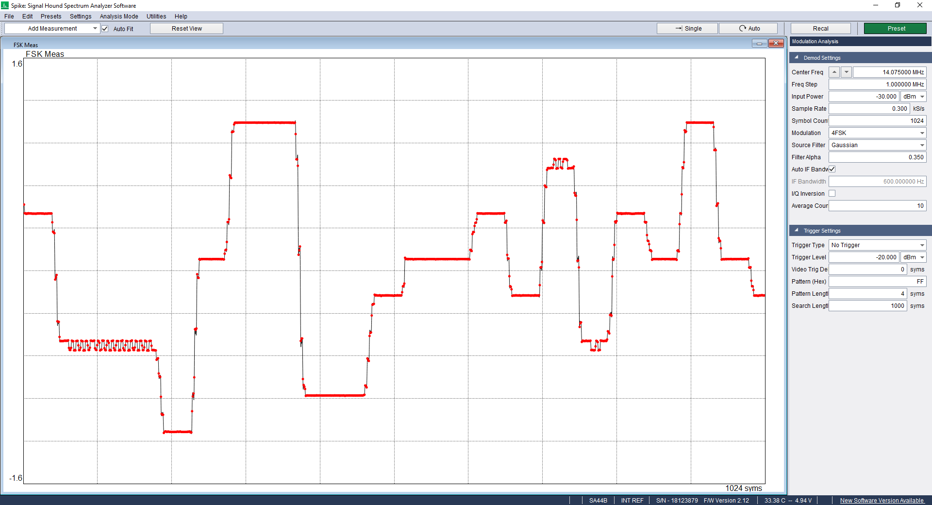
Note the frequency dither, as the QDX can’t decide on which frequency to send. This should have absolutely no impact on performance. 8-FSK FT8 uses a tone-spacing of 6.25 Hz.
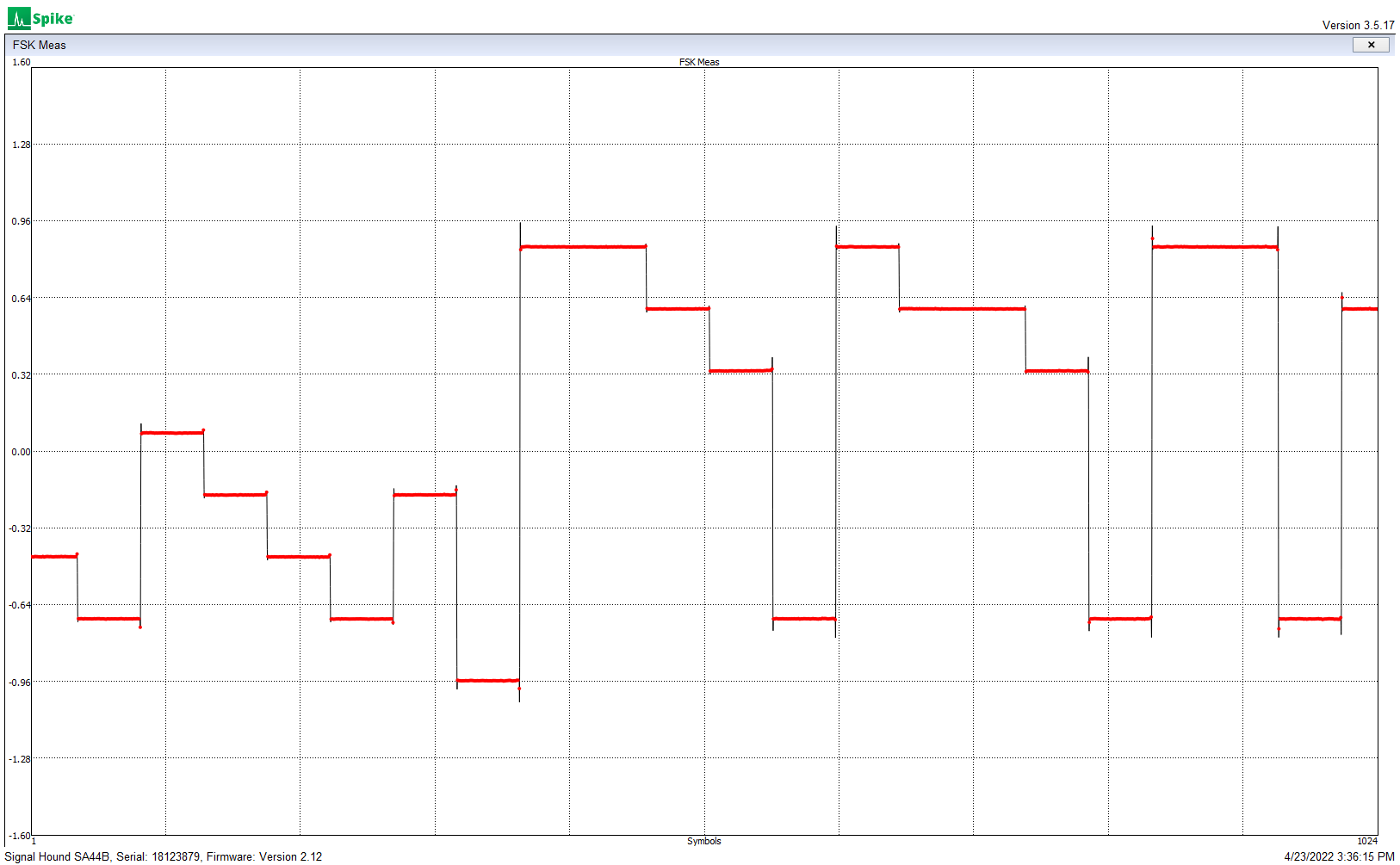
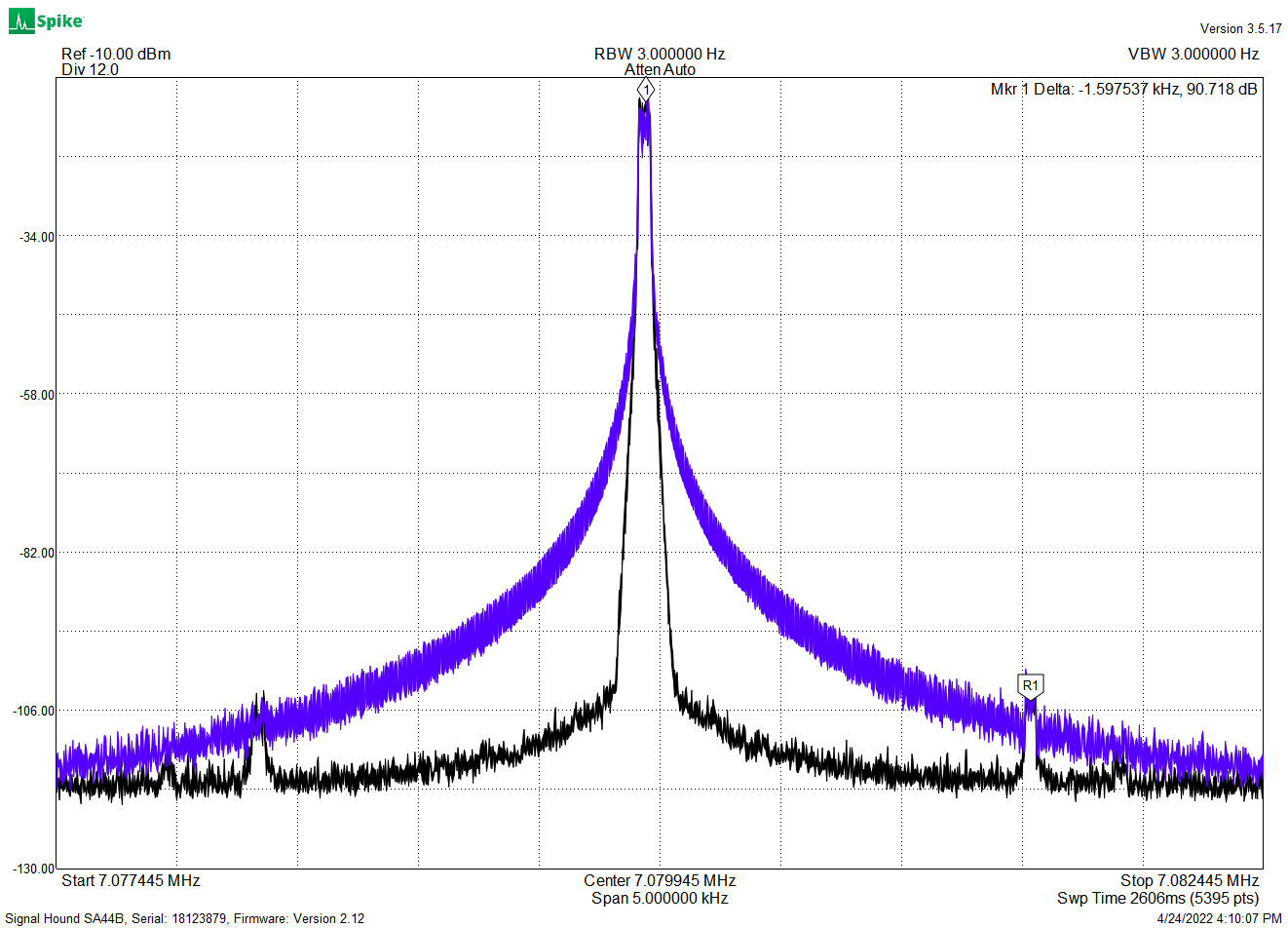
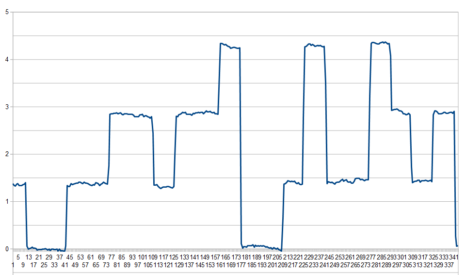
WSPR was next, and there are issues here. The 4-FSK WSPR tone spacing is a narrower 1.456 Hz, and the QDX has difficulty generating these evenly-spaced tones. Here is the analyzer modulation display for 30 meter WSPR:
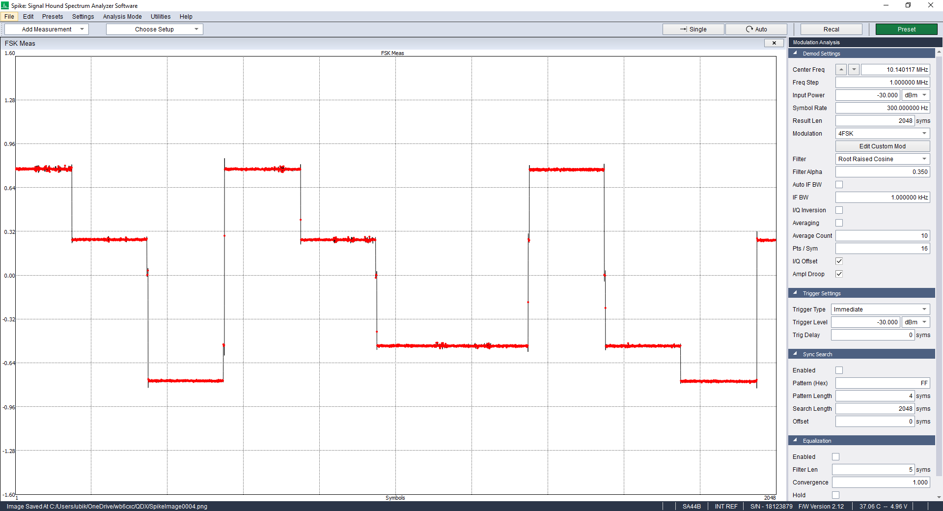
Notice how the tone frequency steps aren’t even. Tone 1 should be halfway between tone 0 and tone 2 (and it isn’t). I wasn’t able to measure exact tone frequencies with the modulation analyzer mode, so I put together a different test setup:
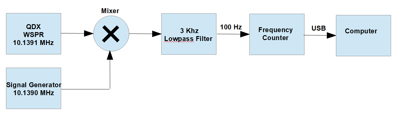
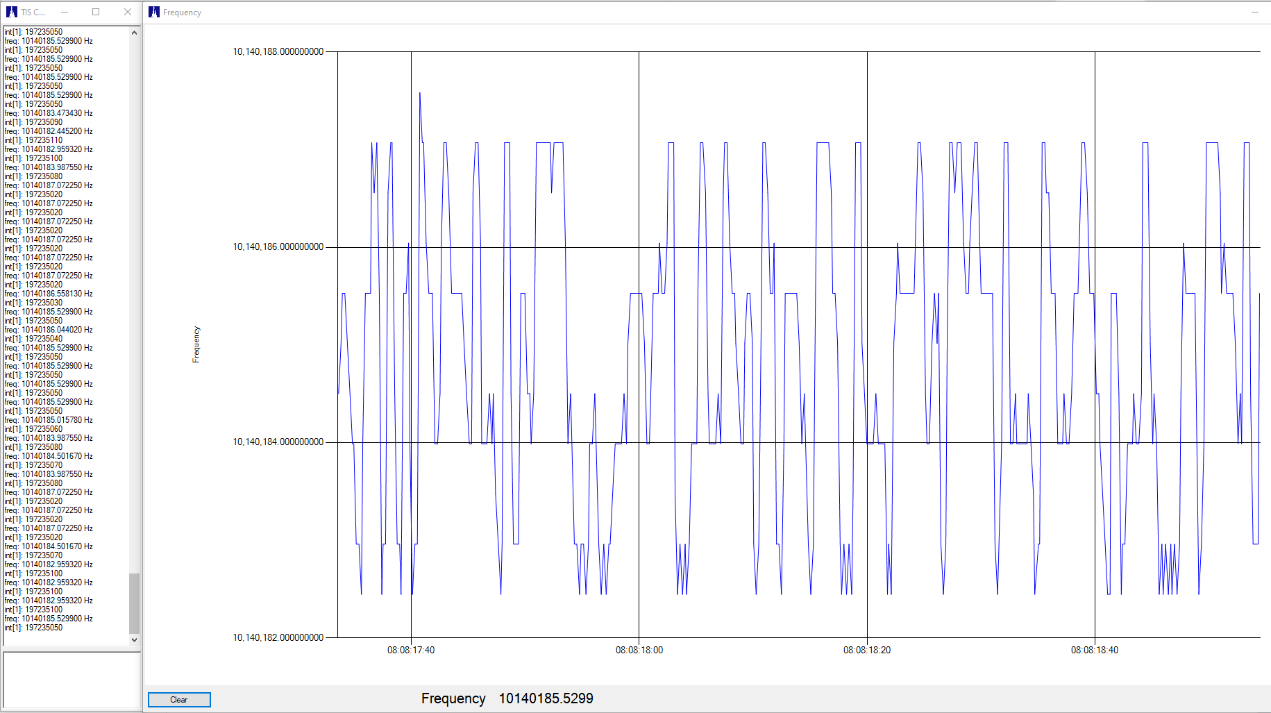
This technique mixes the output of the transmitter with a fixed-frequency signal generator, and the resulting difference frequency can be measured by a frequency counter. I used a Time Interval Counter of my own design that does “reciprocal” counting where the period of the input signal is measured with 10ns resolution, resulting in fast and accurate measurement, especially for low frequency inputs. These measurements are sent to a PC where they can be plotted and analyzed.
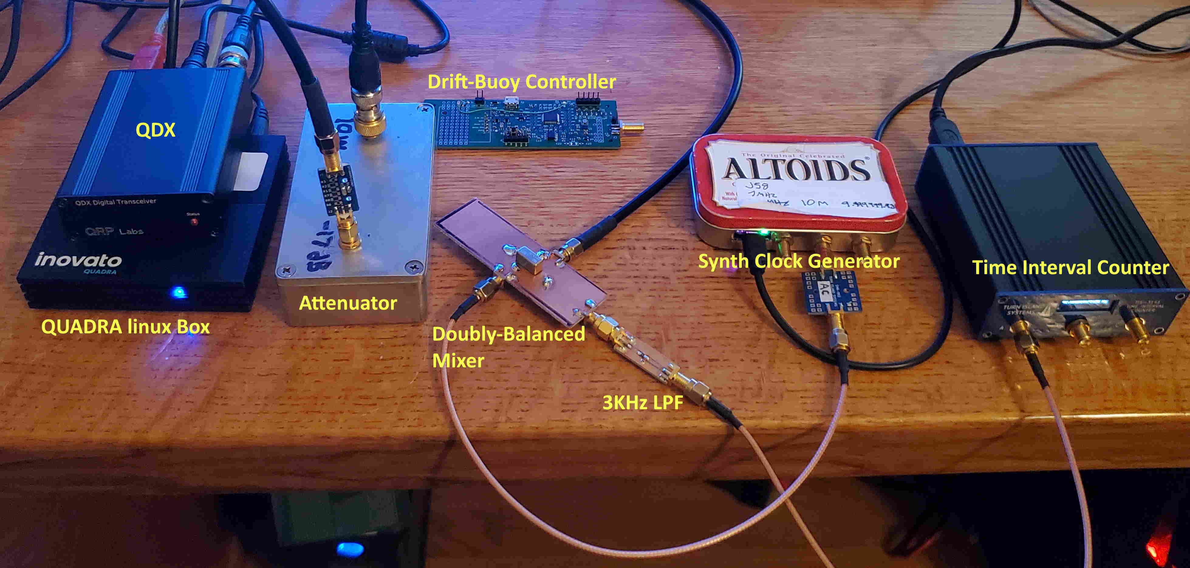
I had all the pieces lying around except for my low-pass filter, for which I put a simple R-C netwotk (470 Ohms series, 0.1uF shunt) and some SMA connectors on a bit of circuit board. That Altoids tin contains a simple Si5351 clock generator, a tiny controller, and a not-particularly-stable crystal oscillator.
So here are some measurement results:
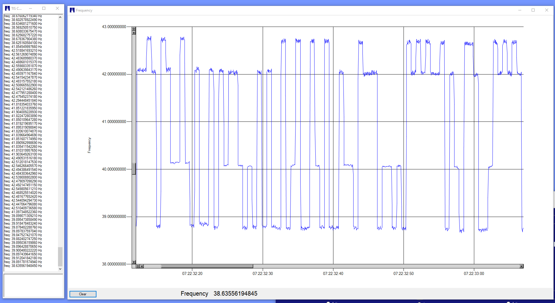
This was done with the mixing generator set about 40 Hz lower than the QDX WSPR transmission. The counter is pre-dividing the 40Hz difference frequency by four, resulting in a measurement rate of about 10Hz. This gives about 14 or 15 samples per WSPR symbol. Here we can see the same problem with the QDX frequency setting — this time it’s Tone 2 that is shifted. The specifics of the shift or frequency error depends on the actual audio frequency coming in to the QDX (sent my WSJTX). Here is the modulation with the WSPR transmit offset at 1404Hz (I believe that slow frequency shift is the QDX as it warms up, but I should test that using a better frequency reference):
Note that the step error is at the low-frequency end. Incrementing the audio frequencies by 1 Hz gives us this with the error at the upper frequency end:
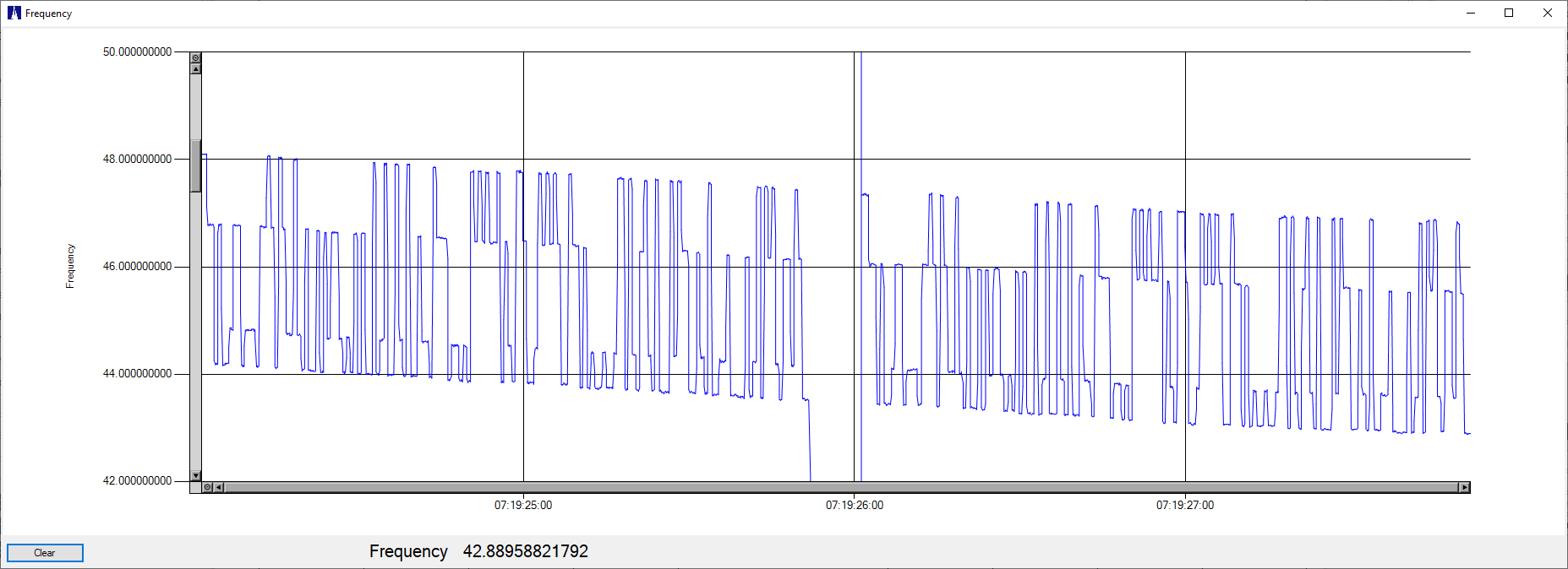
I saw the same error-vs-audio-frequency behavior as when using the spectrum analyzer modulation test. As another check, I used my drift-buoy controller/synthesizer as a WSPR source (here, generating random WSPR -4FSK tones, and the measurements put into a spreadsheet in order to zero-reference the frequencies):
 The tone frequencies are correct.
The QDX displays this WSPR frequency issue on both 30 and 20 meters, and I assume on the other bands as well. I have used the QDX to successfully transmit WSPR, so this amount of error isn’t necessarily critical, but I look forward to enhanced performance in the near future.
For what it’s worth, the Time Interval Counter (TIC) I am using (and designed) is able to directly measure the WSPR modulation at the 10.140… MHz carrier frequency, without using the fancy mixing / down-conversion arrangement:
Here the TIC has pre-divided the 10.xxx MHz input frequency by 2,000,000 which gives us about five measurements per second, about the slowest rate that will reasonably measure 1.456 Hz symbol rate of WSPR. With the 10 ns resolution of the TIC, this results in frequency measurements with about 1/2 Hz resolution. This is good enough to show the modulation, but not good enough to accurately measure it.
The down-conversion method, by directly mixing the 10.xxx MHz signal down to about 100Hz, provides a single-cycle frequency resolution of about 0.0001 Hz. Since I am measuring four cycles, that gives 0.000025 Hz resolution, certainly enough to accurately measure WSPR deviation!
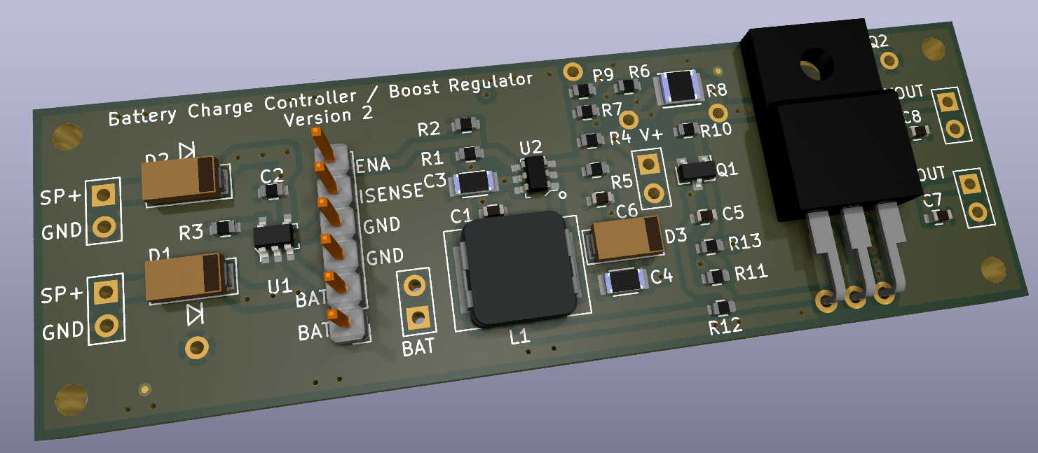
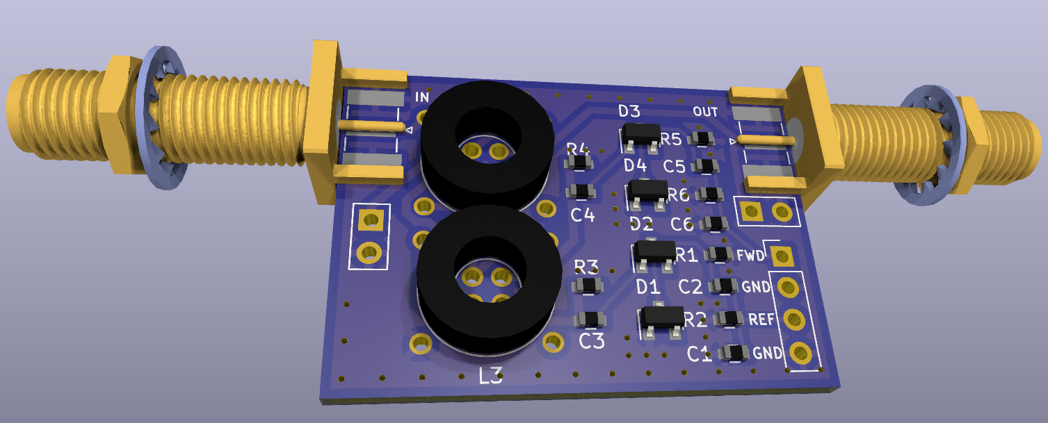 3D KiCad Rendering
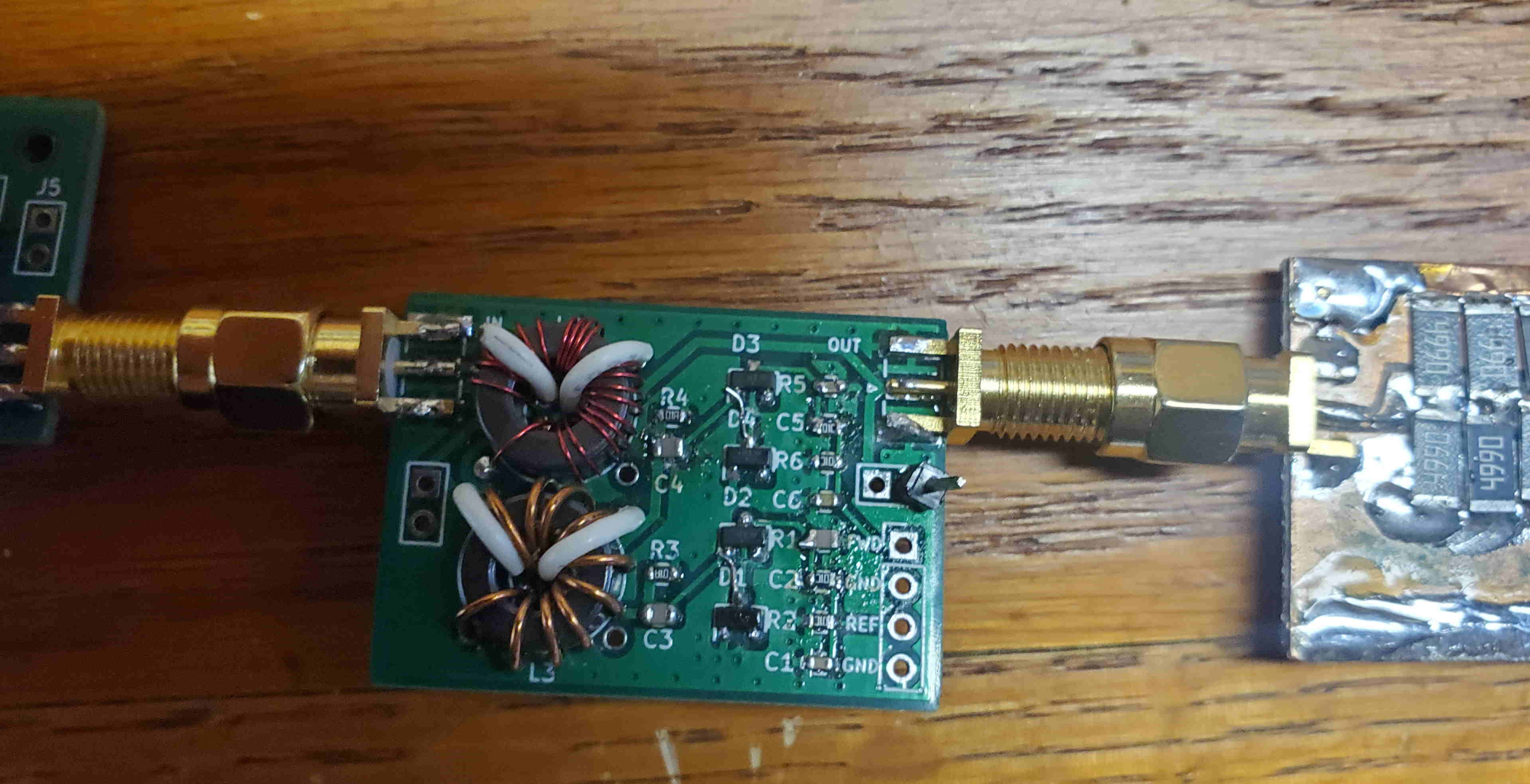
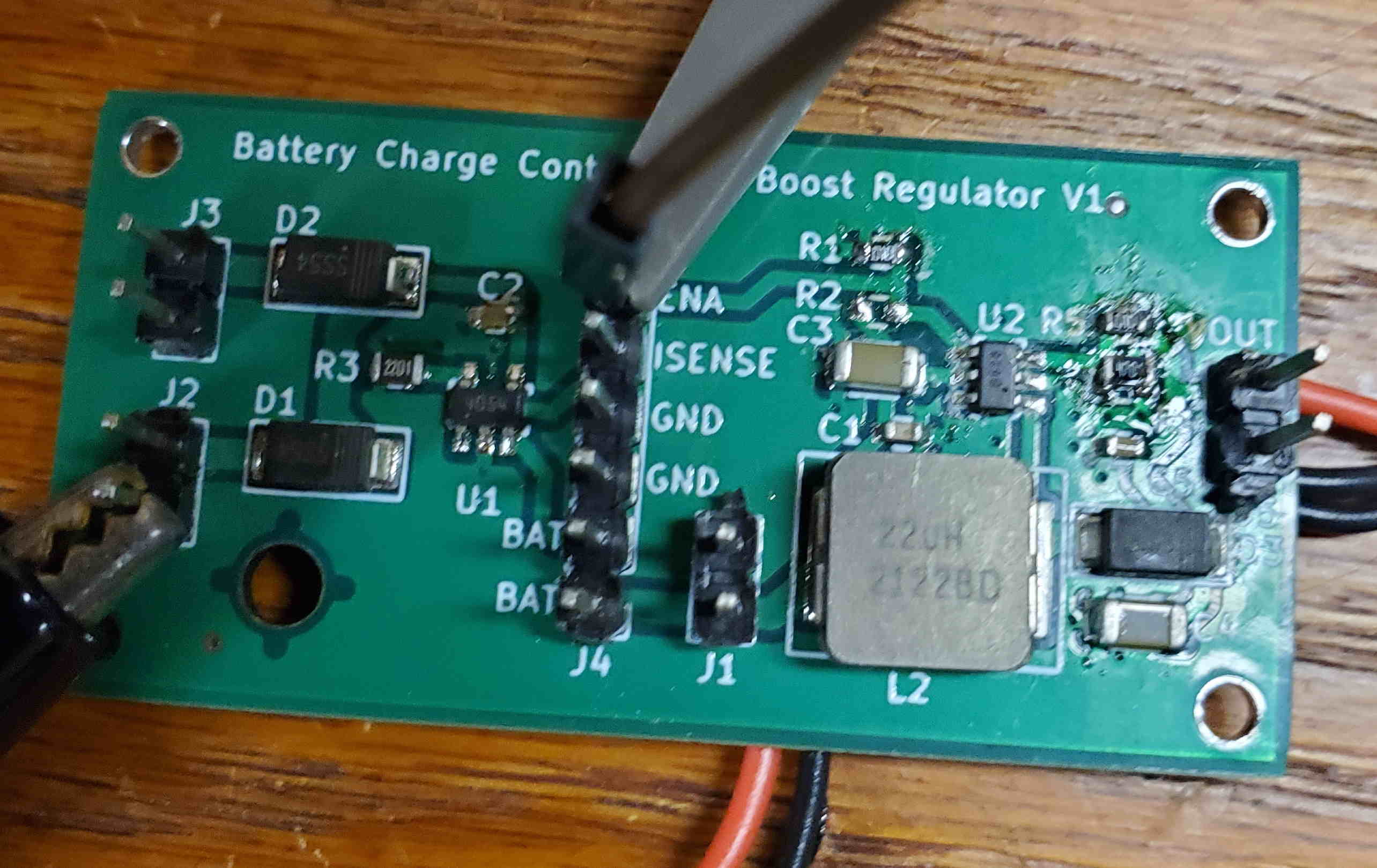 (I need to clean off that scorched flux!)
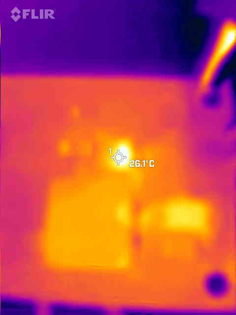 Thermal Scan
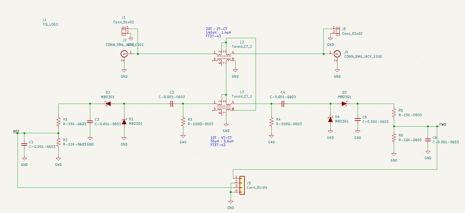
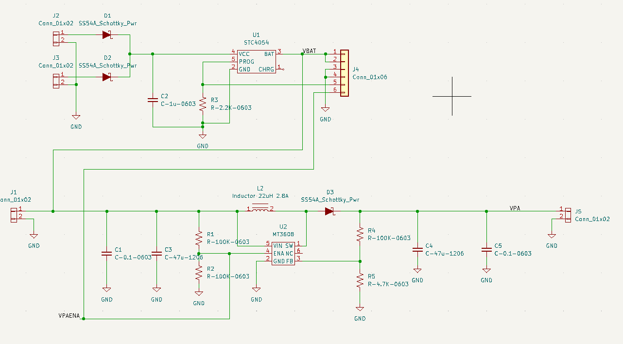
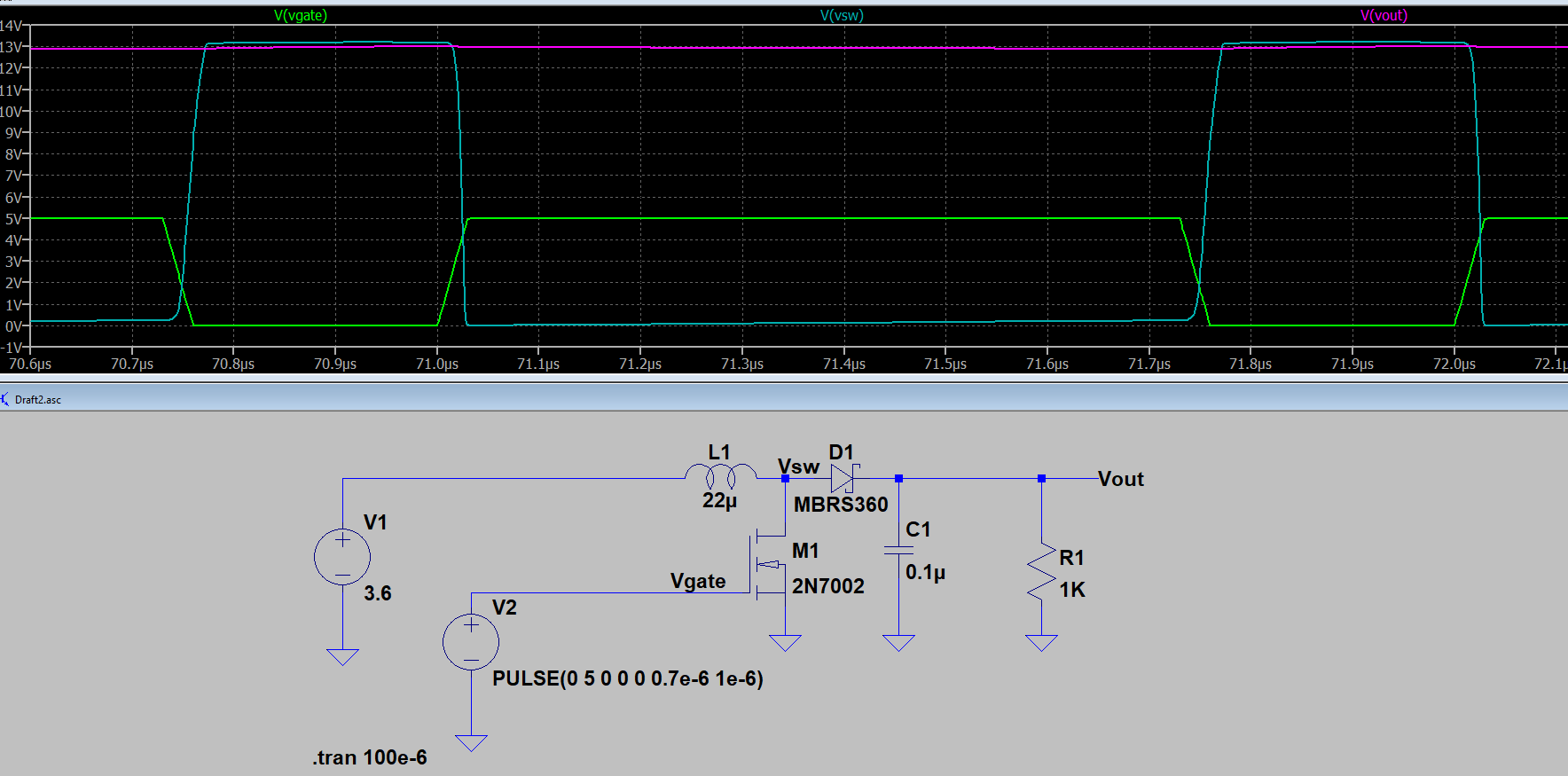 Essential Boost Converter Circuit
 Low-Voltage Shutoff Circuit